Check patentability & draft patents in minutes with Patsnap Eureka AI!

Pre-silicide spacer removal

a spacer and pre-silicide technology, applied in the field of semiconductor spacer removal, can solve the problems of limiting the effectiveness of stress transfer to the channel, inadequate room for good contact, adversely affecting subsequent processes, etc., and achieve the effect of limiting the effectiveness of stress transfer and insufficient room

Inactive Publication Date: 2008-04-17
INFINEON TECH AG +2
View PDF10 Cites 4 Cited by
  • Summary
  • Abstract
  • Description
  • Claims
  • Application Information

AI Technical Summary

Benefits of technology

[0002]In transistors, a gate sidewall spacer is generally used to space the source / drain diffusions and silicide away from the device channel region (the shallow extension implant bridges the gap). Once silicide is formed, the spacer is typically left in place where it may adversely affect subsequent processes. For example, the spacer crowds the limited area between closely spaced gates leaving inadequate room to form good contacts. Also, the presence of the spacer forces the stress liner further from the device channel thereby limiting the effectiveness of stress transfer to the channel.
[0006]Following this, the method deposits a mask over the gate conductor, the spacers, and the source and drain regions. Following this the mask is recessed to a level below a top of the gate conductor, but above the source and drain regions, such that a portion of the spacers are exposed and the source and drain regions are protected by the mask. With the mask in place, the method then safely removes the spacers and the gate cap, without damaging the source / drain regions or the isolation regions (which are protected by the mask). Next, the method removes the mask and then forms silicide regions on the gate conductor and the source and drain regions. This leaves a structure with silicided gate conductor and source / drain regions and no spacers next to the gate conductor.

Problems solved by technology

Once silicide is formed, the spacer is typically left in place where it may adversely affect subsequent processes.
For example, the spacer crowds the limited area between closely spaced gates leaving inadequate room to form good contacts.
Also, the presence of the spacer forces the stress liner further from the device channel thereby limiting the effectiveness of stress transfer to the channel.
The problem with simply stripping the nitride spacer after silicide formation is that etchants suitable for nitride removal also erode silicide.
Use of a sacrificial nitride deposited preferentially on the silicide has been attempted but the beneficial effect of protecting the silicide tends to be overwhelmed by the need to etch longer to remove both the spacer and the additional nitride from the gate sidewall.
Removal of this cap nitride with exposed silicon and SiGe results in uncontrolled recess of the silicon and SiGe since nitride etchants typically have poor selectivity to silicon and SiGe.

Method used


Image

  • Pre-silicide spacer removal
  • Pre-silicide spacer removal
  • Pre-silicide spacer removal

Examples


Embodiment Construction

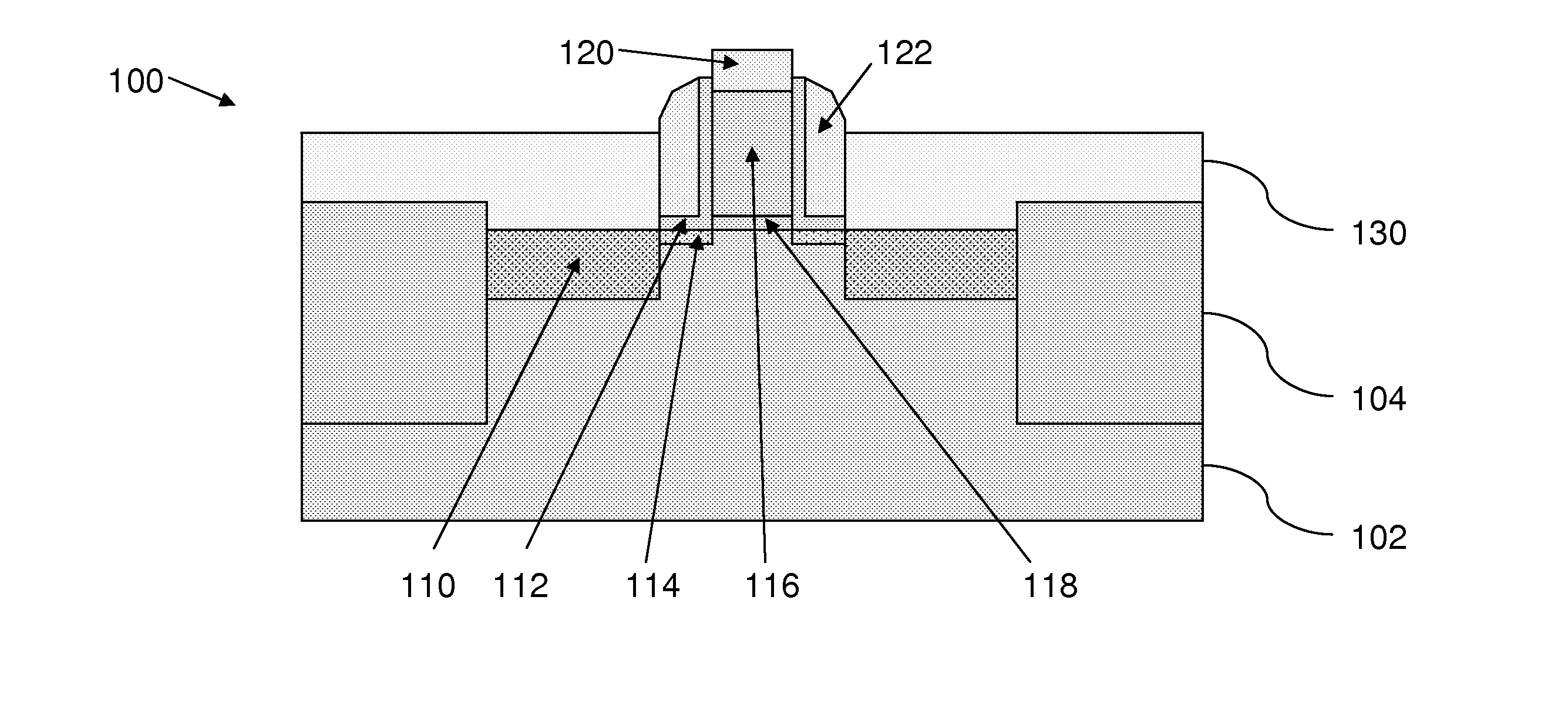
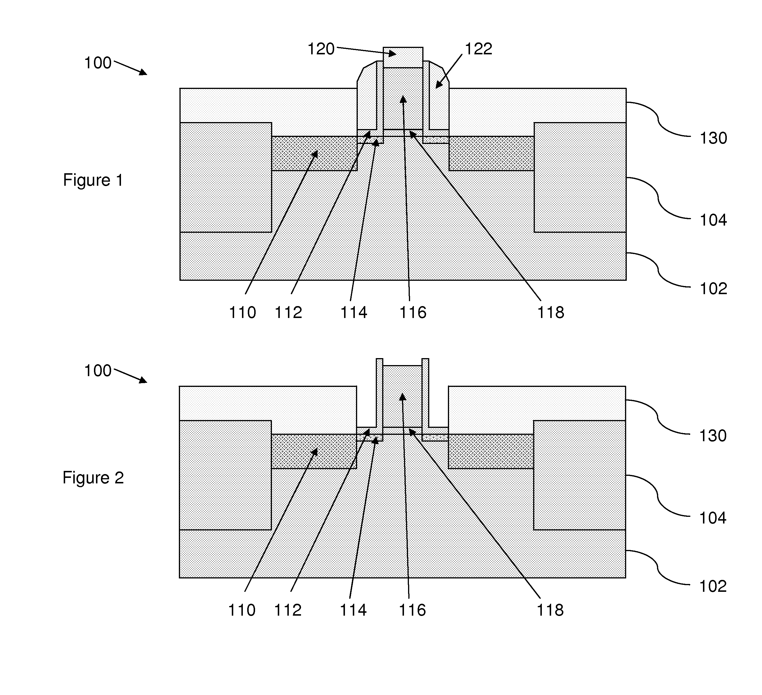
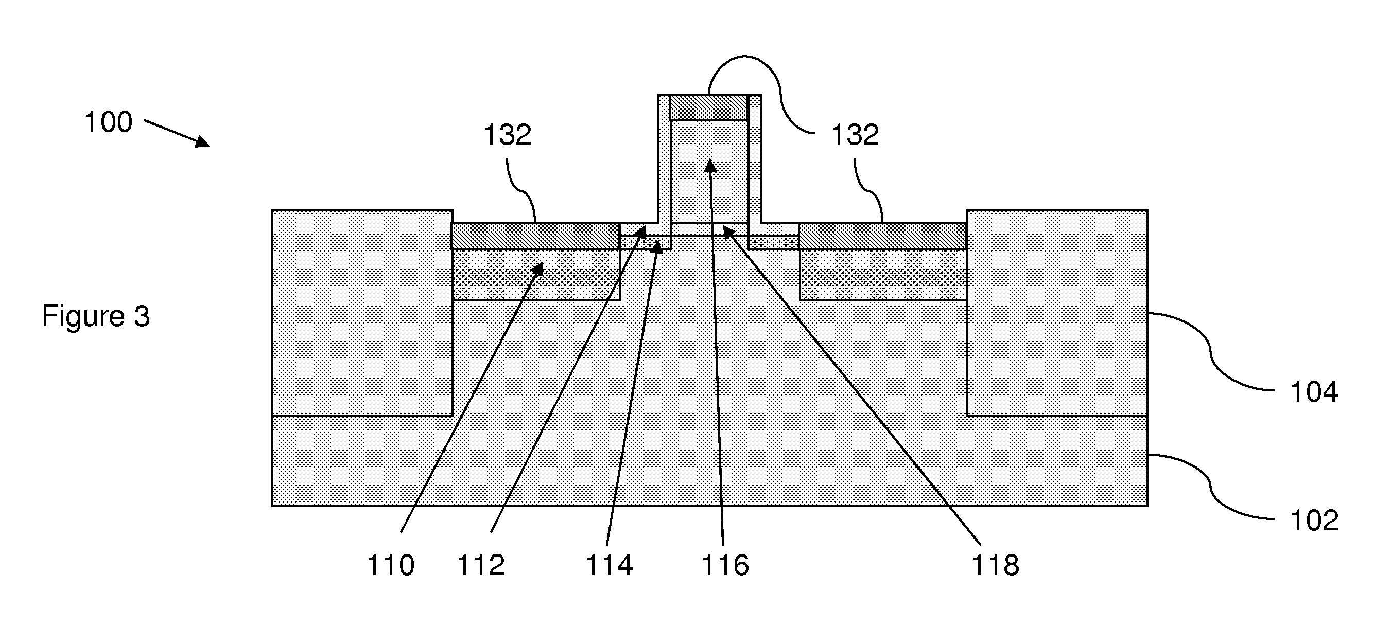
[0012]The embodiments of the invention and the various features and advantageous details thereof are explained more fully with reference to the non-limiting embodiments that are illustrated in the accompanying drawings and detailed in the following description. It should be noted that the features illustrated in the drawings are not necessarily drawn to scale. Descriptions of well-known components and processing techniques are omitted so as to not unnecessarily obscure the embodiments of the invention. The examples used herein are intended merely to facilitate an understanding of ways in which the embodiments of the invention may be practiced and to further enable those of skill in the art to practice the embodiments of the invention. Accordingly, the examples should not be construed as limiting the scope of the embodiments of the invention.

[0013]As discussed above, the problem with simply stripping the nitride spacer after silicide formation is that etchants suitable for nitride re...


PUM


Abstract

A method forms a gate conductor over a substrate, and simultaneously forms spacers on sides of the gate conductor and a gate cap on the top of the gate conductor. Isolation regions are formed in the substrate and the method implants an impurity into exposed regions of the substrate not protected by the gate conductor and the spacers to form source and drain regions. The method deposits a mask over the gate conductor, the spacers, and the source and drain regions. The mask is recessed to a level below a top of the gate conductor but above the source and drain regions, such that the spacers are exposed and the source and drain regions are protected by the mask. With the mask in place, the method then safely removes the spacers and the gate cap, without damaging the source / drain regions or the isolation regions (which are protected by the mask). Next, the method removes the mask and then forms silicide regions on the gate conductor and the source and drain regions.

Description

BACKGROUND AND SUMMARY[0001]The embodiments of the invention generally relate to transistor manufacturing and more particularly to a method of removing sidewall spacers before silicide has been formed.[0002]In transistors, a gate sidewall spacer is generally used to space the source / drain diffusions and silicide away from the device channel region (the shallow extension implant bridges the gap). Once silicide is formed, the spacer is typically left in place where it may adversely affect subsequent processes. For example, the spacer crowds the limited area between closely spaced gates leaving inadequate room to form good contacts. Also, the presence of the spacer forces the stress liner further from the device channel thereby limiting the effectiveness of stress transfer to the channel.[0003]The problem with simply stripping the nitride spacer after silicide formation is that etchants suitable for nitride removal also erode silicide. Use of a sacrificial nitride deposited preferentia...

Claims


Application Information

Patent Timeline
Patent Type & Authority Applications(United States)
IPC IPC(8): H01L21/44
CPCH01L21/32H01L29/665H01L29/6659H01L29/66545H01L29/6653H01L21/18H01L21/24
Inventor DYER, THOMAS W.FANG, SUNFEIYAN, JIANGKIM, JUN JUNGLIU, YAOCHENGZHU, HUILONG
Owner INFINEON TECH AG
Features
  • R&D
  • Intellectual Property
  • Life Sciences
  • Materials
  • Tech Scout
  • Unparalleled Data Quality
  • Higher Quality Content
  • 60% Fewer Hallucinations
Learn More