Reduced leakage interconnect structure

a leakage-reducing and interconnecting technology, applied in the field of backend of the line (beol) interconnect structure, can solve the problems of increasing the concern of reliability, increasing the problem of leakage, and reducing the spacing of wires to wires

Active Publication Date: 2008-05-01
GLOBALFOUNDRIES US INC
View PDF22 Cites 28 Cited by
  • Summary
  • Abstract
  • Description
  • Claims
  • Application Information

AI Technical Summary

Benefits of technology

[0013]The semiconductor device further comprises a second dielectric layer in contact with the dielectric capping layer. The first dielectric layer prefe

Problems solved by technology

The continuous scaling to smaller dimensions and the introduction of low-k dielectrics in copper interconnects have caused reliability issues to become a greater concern in addition to increasing process complexity.
Chemical Mechanical Polish (CMP) residues may cause wire to wire electrical shorts.
This problem is becoming more serious as the wire to wire spacing is decreased.
It has been observed that post CMP Cu scratches and/or residue between interconnects are a major cause of dielectric breakdown failure.
This dielectric breakdown failure is a reliability issue which is getting worse as IC critical dimensions continue to scale down.
EM is a serious reliability concern for very large scale integrated (VLSI) circuits.
This can result in a circuit dead

Method used


Image

  • Reduced leakage interconnect structure
  • Reduced leakage interconnect structure
  • Reduced leakage interconnect structure

Examples


Embodiment Construction

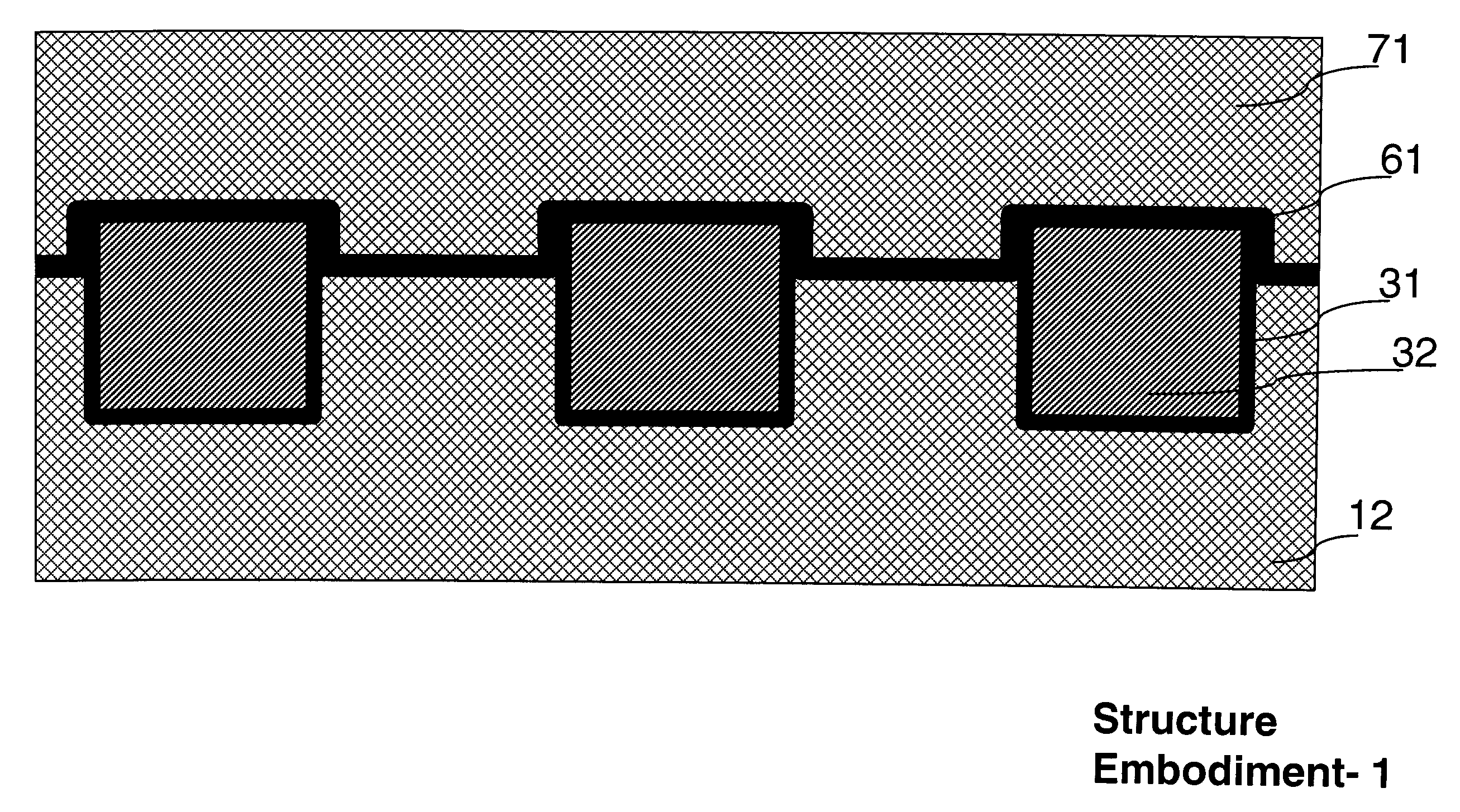
[0025]The present invention provides an interconnect structure comprising a recessed dielectric layer which reduces embedded metallic residues from CMP scratches and metal cap applications and provides improved mechanical integrity at the cap / liner / dielectric junction.

[0026]According to the present invention, a semiconductor interconnect structure is provided that includes a new capping layer / dielectric material interface which is embedded inside the dielectric material. In particular, the new interface is located in the upper surface of a dielectric material that is adjacent to a conductive region or feature. The presence of the dielectric material that is adjacent to the conductive region or feature provides a new interface that has a high mechanical strength and improved reliability. Further, the new interface provided in the present invention is free of metal residues and has a high dielectric breakdown resistance which is important for future technology extendibility. Further, ...


PUM


Abstract

An improved semiconductor device interconnect structure comprising a dielectric layer recessed with respect to the conductive interconnect features. This structure and method reduces embedded metallic residues from CMP scratches and metal cap applications and provides improved mechanical integrity at the capping layer/liner/dielectric interface.

Description

BACKGROUND OF THE INVENTION[0001]The present invention relates to semiconductor integrated circuits (ICs), and more particularly to a back-end-of-the-line (BEOL) interconnect structure.[0002]The continuous scaling to smaller dimensions and the introduction of low-k dielectrics in copper interconnects have caused reliability issues to become a greater concern in addition to increasing process complexity. Chemical Mechanical Polish (CMP) residues may cause wire to wire electrical shorts. This problem is becoming more serious as the wire to wire spacing is decreased.[0003]It has been observed that post CMP Cu scratches and / or residue between interconnects are a major cause of dielectric breakdown failure. This dielectric breakdown failure is a reliability issue which is getting worse as IC critical dimensions continue to scale down.[0004]In semiconductor interconnect structures, electromigration (EM) has been identified as a metal failure mechanism. EM is a serious reliability concern ...

Claims


Application Information

Patent Timeline
IPC IPC(8): H01L21/76H01L29/40H01L29/06
CPCH01L21/76834H01L21/76885H01L21/76849
Inventor YANG, CHIH-CHAO
Owner GLOBALFOUNDRIES US INC
Why Eureka
Try Eureka