Electronic device including a transistor having a metal gate electrode and a process for forming the electronic device

a technology of electronic devices and metal gate electrodes, applied in the direction of semiconductor devices, electrical equipment, transistors, etc., can solve the problems of high cost and complexity trade-offs on a manufacturing line, where a mixture of highly integrated products with different requirements is made, and can be particularly problematic and expensive, and long processes that are both time-consuming and expensive to perform, and add complexity to both imaging and planarization processing during manufacturing

Inactive Publication Date: 2008-05-15
NORTH STAR INNOVATIONS
View PDF16 Cites 30 Cited by
  • Summary
  • Abstract
  • Description
  • Claims
  • Application Information

AI Technical Summary

Problems solved by technology

Thus managing cost and complexity trade-offs on a manufacturing line where a mixture of highly integrated products with different requirements are made can be particularly problematic and expensive.
Ho

Method used


Image

  • Electronic device including a transistor having a metal gate electrode and a process for forming the electronic device
  • Electronic device including a transistor having a metal gate electrode and a process for forming the electronic device
  • Electronic device including a transistor having a metal gate electrode and a process for forming the electronic device

Examples


Embodiment Construction

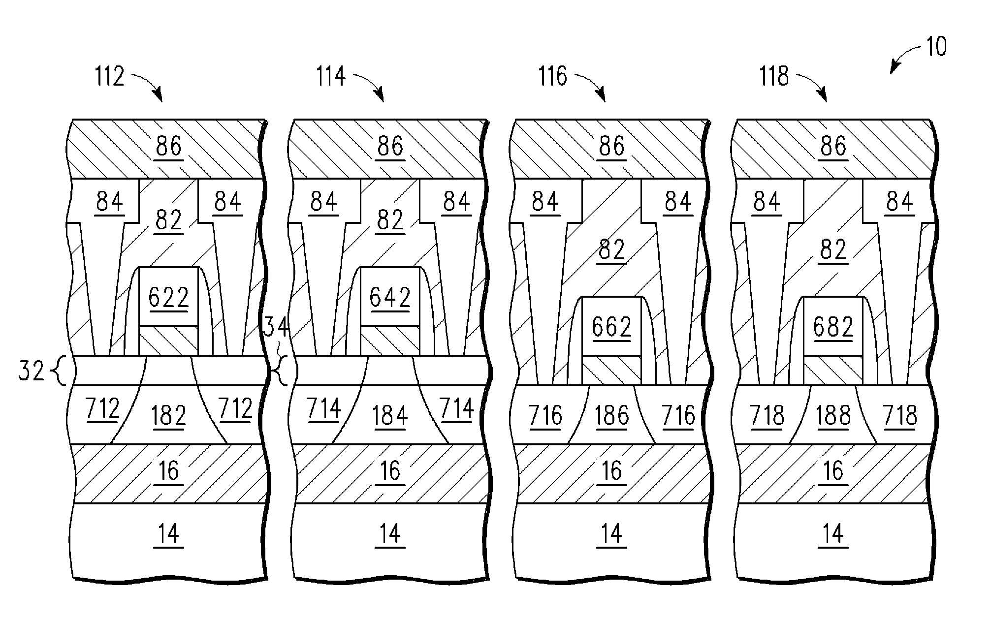
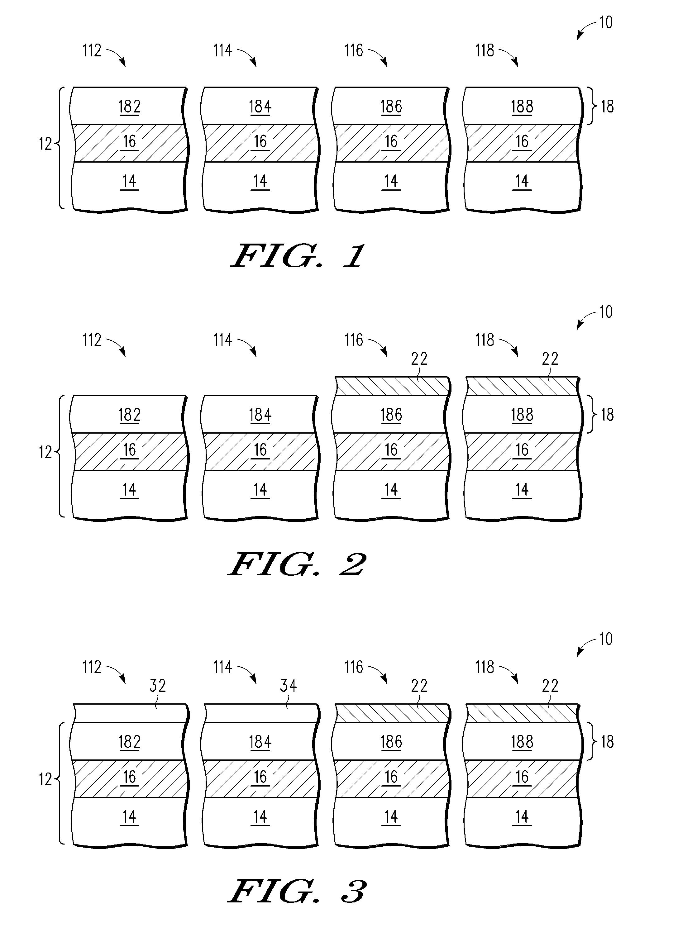
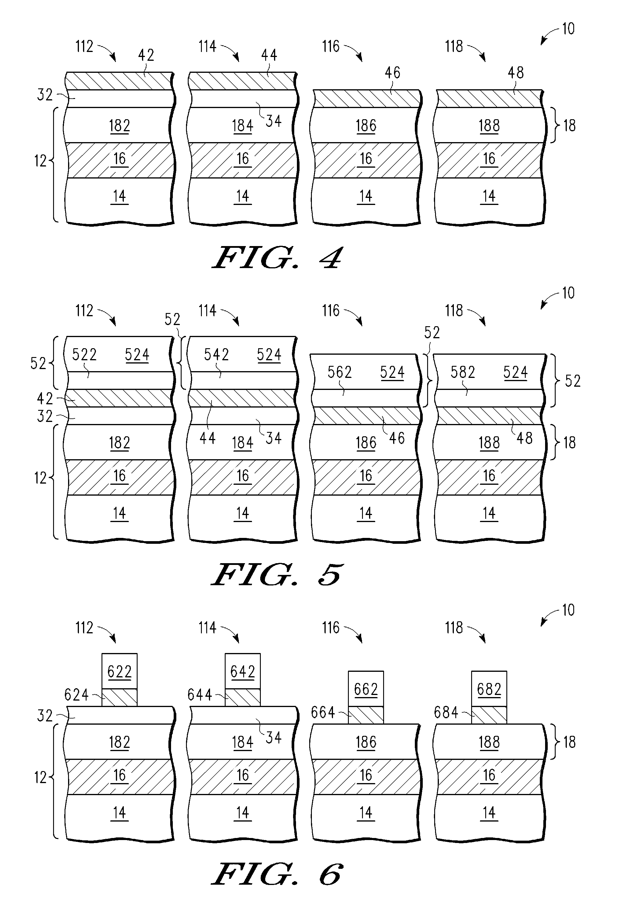
[0018]An electronic device includes an n-channel and a first p-channel transistor having a first gate electrode with a first work function and a first channel region including a semiconductor layer immediately adjacent to a semiconductor substrate. In a first aspect, the first p-channel transistor includes the first channel region and the semiconductor layer lying immediately adjacent to the semiconductor substrate. The semiconductor substrate can have a first semiconductor composition. The semiconductor layer has a second semiconductor composition different from the first semiconductor composition, and the semiconductor layer has a thickness of at most approximately 10 nm. The first p-channel transistor can also include a first metal gate electrode associated with the first channel region and having a first work function less than a valence band of the semiconductor layer.

[0019]In a second aspect, the first transistor is a p-channel transistor and the electronic device can also inc...


PUM


Abstract

An electronic device includes an n-channel transistor and a p-channel transistor. The p-channel transistor has a first gate electrode with a first work function and a first channel region including a semiconductor layer immediately adjacent to a semiconductor substrate. In one embodiment, the first work function is less than the valence band of the semiconductor layer. In another embodiment, the n-channel transistor has a second gate electrode with a second work function different from the first work function and closer to a conduction band than a valence band of a second channel region. A process of forming the electronic device includes forming first and second gate electrodes having first and second work functions, respectively. First and second channel regions having a same minority carrier type are associated with the first and second gate electrodes, respectively.

Description

RELATED APPLICATION[0001]The present disclosure relates to U.S. patent application Ser. No. ______, entitled “Electronic Device Including a Heterojunction Region and a Process for Forming the Electronic Device” by Winstead, et. al. filed on ______, 2006 (Attorney Docket Number MT10305TP), which is assigned to the current assignee hereof and incorporated by reference in its entirety.BACKGROUND[0002]1. Field of the Disclosure[0003]The present disclosure relates to electronic devices, more particularly, to electronic devices that include transistors having metal gate electrodes and a process for forming them.[0004]2. Description of the Related Art[0005]Many semiconductor manufacturing facilities run a mixture of products with different requirements in order to remain full and profitable. Thus managing cost and complexity trade-offs on a manufacturing line where a mixture of highly integrated products with different requirements are made can be particularly problematic and expensive.[00...

Claims


Application Information

Patent Timeline
IPC IPC(8): H01L27/088H01L21/77
CPCH01L21/823807H01L29/1054H01L21/823842
Inventor CAPASSO, CRISTIANOSAMAVEDAM, SRIKANTH B.VERRET, ERIC J.
Owner NORTH STAR INNOVATIONS
Why Eureka
Try Eureka