Semiconductor generation of dynamic infrared images
Inactive Publication Date: 2006-08-01
US SEC THE AIR FORCE THE
View PDF11 Cites 32 Cited by
Summary
Abstract
Description
Claims
Application Information
AI Technical Summary
This helps you quickly interpret patents by identifying the three key elements:
Problems solved by technology
Method used
Benefits of technology
[0006]The present invention provides a semiconductor transducer-based high-speed, high-resolution
Problems solved by technology
Experience has shown that a large scale outdoor environment does not offer the repeatability or controllability of test conditions needed for the development of, or the testing and maintenance of, such equipment.
However, thermal resistor arrays suffer from long time constants, often involving respons
Method used
Image
Click on the blue label to locate the original text in one second.
Reading with bidirectional positioning of images and text.
Examples
example class 1
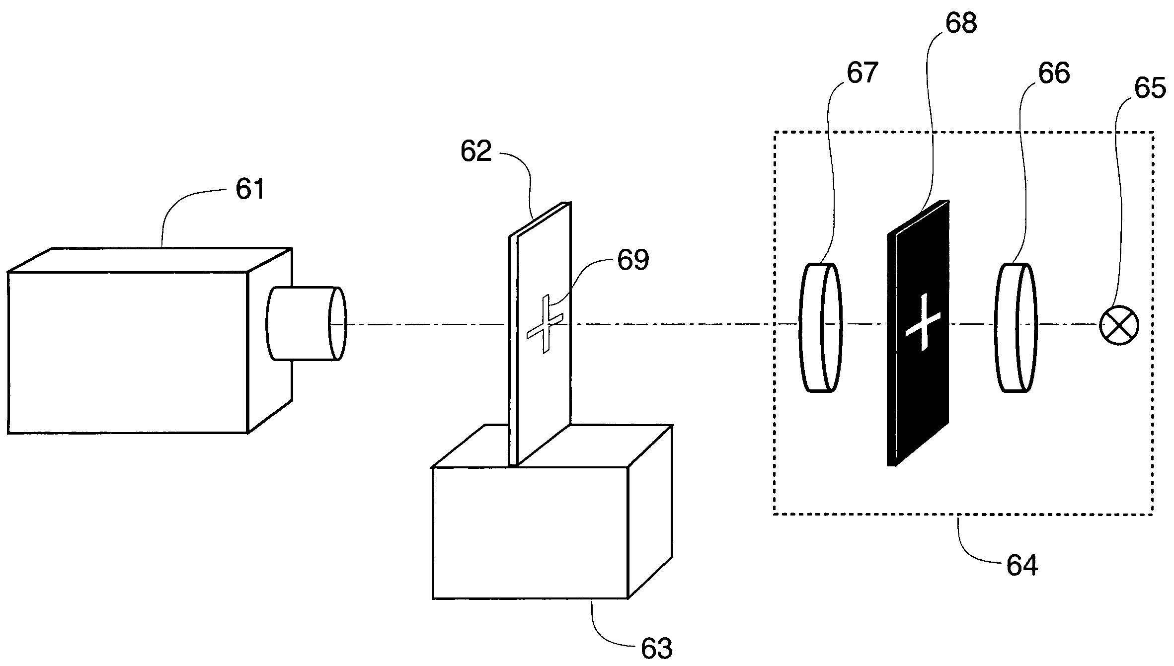
Germanium in a FIG. 1 Semiconductor Screen
Infrared Outputs in the 8 to 12 Micrometers Wavelength Range
[0073]For this example class an n-doped sample of optically transparent homopolar Germanium semiconductor having an electrical resistivity, ρ, value between 0.1 and 45 ohm-cm is used. The element Antimony, Sb, is used as an n-dopant in this material. Doping at this level is a compromise between infrared transparency and intrinsic hole concentration providing minimum initial natural emissivity when heated. The needed doping level is screen operating-temperature dependent. Doping is achieved during crystal growth using a classic Chohralski or Bridgment process. Such doping of Germanium semiconductor material to achieve transparency is described in the technical journal paper “Absorption Coefficient of Ge at 10.6 mkm” authored by P. Bishop and A. Gibson, Applied Optics, volume 12, number 11, pages 2549–2550, 1973; the contents of this paper are also hereby incorporated by reference her...
example class 2
Silicon in a FIG. 1 Semiconductor Screen
Infrared Outputs in the 3 to 5 Micrometers Wavelength Range
[0081]2a. Si n-doped, ρ=500 Ohm.cm, τ=2.5 milliseconds, T=240° C., 14.4×20.5×8.4 mm3 dimensions. T1=86° C. and T2=190° C., ΔT=104° C.
[0082]2b. Si p-doped, ρ=11000 Ohm.cm, τ=1 millisecond, T=232° C., 17.2×18×9.2 mm3 dimensions. T1=86.2° C. and T2=164° C., ΔT=77.8° C.
[0083]The following additional disclosure concerning our present invention includes portions in repetition of parts of the above discussion as well as portions complementary to the above discussion; it is therefore believed helpful in achieving complete theoretical and practical understandings of the invention.
[0084]In the present invention the non-equilibrium infrared thermal emission power of a scene generated in a doped semiconductor plate takes place in a spectral region beyond the fundamental absorption range (the absorbed quantum, ωg, where Eg is the forbidden gap value). Additionally, the apparent temperature scene te...
PUM
Abstract
A high-speed, high-resolution, broadband dynamic infrared scene generator based on semiconductor transducer conversion of visible spectrum scene images into infrared spectrum images. Wavelength conversion is accomplished in the semiconductor material through absorption of visible spectrum energy by valence electrons in a subsurface layer of the semiconductor material and photogeneration by valence band to conduction band electron transfer occurring within about one diffusion length of the semiconductor material surface. The semiconductor material used, for example Germanium or Silicon provides a band gap energy value that is smaller than the quantum energy level of the optical emission. Temperature of the semiconductor material may be maintained at a selected level above or below that of the infrared scene. Infrared images of higher frequency content than are achievable with conventional thermal heating infrared converters are accomplished. The invention thus includes down conversion of visible generated light in order to develop a semiconductor pixel-less Dynamic Infrared Scene Projector capable of simulating high-speed broadband IR scenery.
Description
CLAIM OF PRIORITY[0001]This application claims the benefit of U.S. Provisional Patent Application No. 60 / 490,333, filed Jul. 25, 2003. The contents of this provisional application are hereby incorporated by reference herein.RIGHTS OF THE GOVERNMENT[0002]The invention described herein may be manufactured and used by or for the Government of the United States for all governmental purposes without the payment of any royalty.BACKGROUND OF THE INVENTION[0003]The generation of synthetic infrared scenery is desirable for testing and calibrating of infrared devices. Night vision apparatus is a notable example of such devices finding significant military usage in current world events. Experience has shown that a large scale outdoor environment does not offer the repeatability or controllability of test conditions needed for the development of, or the testing and maintenance of, such equipment. For these reasons, since the early 1990's there has been significant progress in developing synthet...
Claims
Application Information
Patent Timeline
Application Date:The date an application was filed.
Publication Date:The date a patent or application was officially published.
First Publication Date:The earliest publication date of a patent with the same application number.
Issue Date:Publication date of the patent grant document.
PCT Entry Date:The Entry date of PCT National Phase.
Estimated Expiry Date:The statutory expiry date of a patent right according to the Patent Law, and it is the longest term of protection that the patent right can achieve without the termination of the patent right due to other reasons(Term extension factor has been taken into account ).
Invalid Date:Actual expiry date is based on effective date or publication date of legal transaction data of invalid patent.
IPC IPC(8): G21G4/00H01L31/00
CPCH04N17/002H04N5/33
Inventor MALYUTENKO, VOLODYMYR K.KIRCHER, JAMES R.MURRER, JR., ROBERT L.SNYDER, III, DONALD R.MALYUTENKO, OLEG Y.BOGATYRENKO, VYACHESLAV V.