

Semiconductor device having a pair of fins and method of manufacturing the same
a technology of semiconductor and fin, which is applied in the direction of semiconductor devices, semiconductor/solid-state device details, electrical apparatus, etc., can solve the problems of relatively expensive soi substrates, etc., and achieve the effect of reducing short channel effect, and reducing disturbances during reading operations
- Summary
- Abstract
- Description
- Claims
- Application Information
AI Technical Summary
Benefits of technology
Problems solved by technology
Method used
Image

Examples
Embodiment Construction
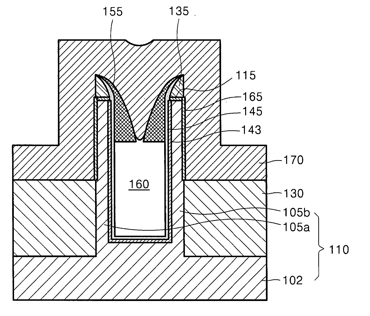
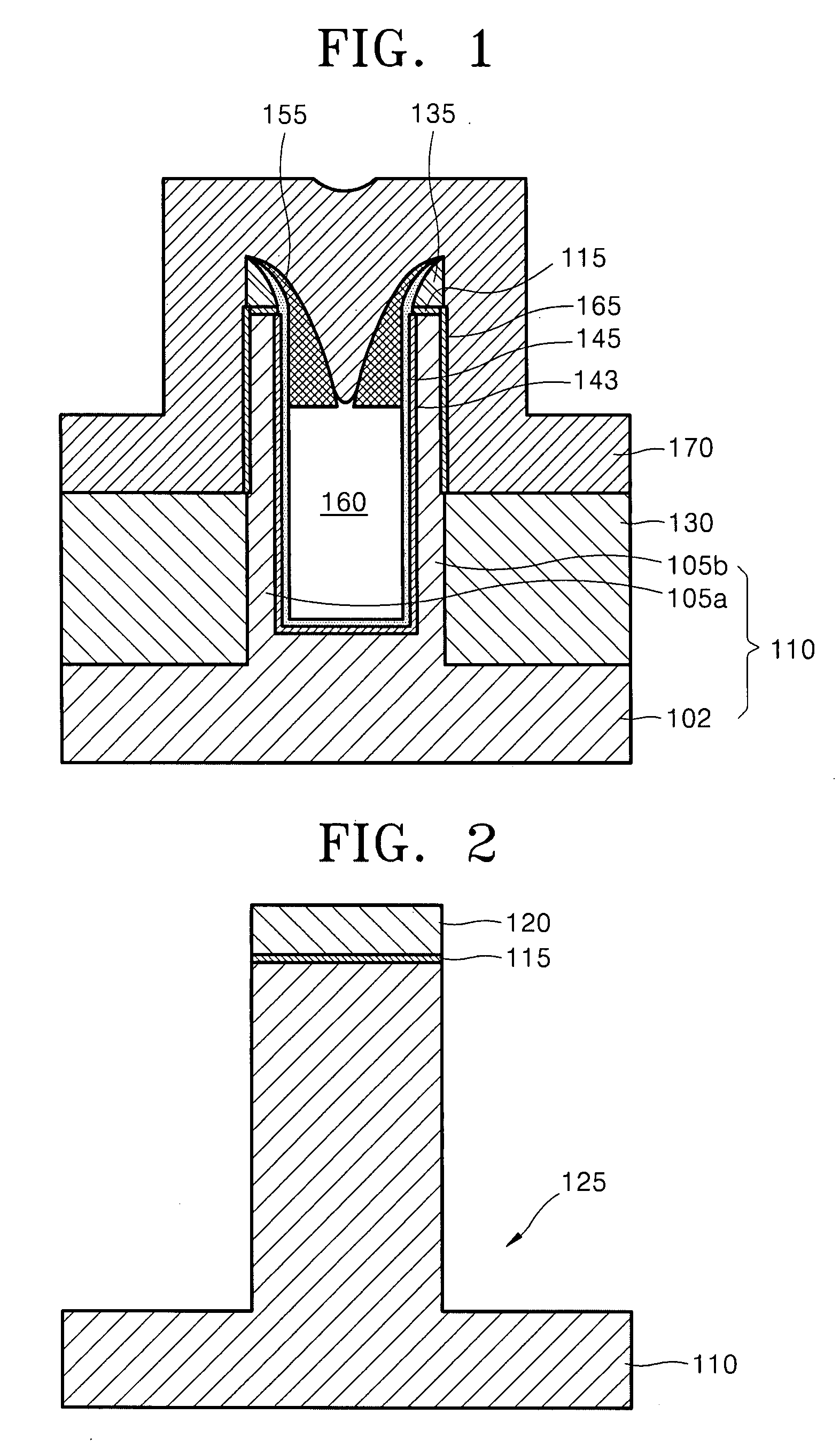
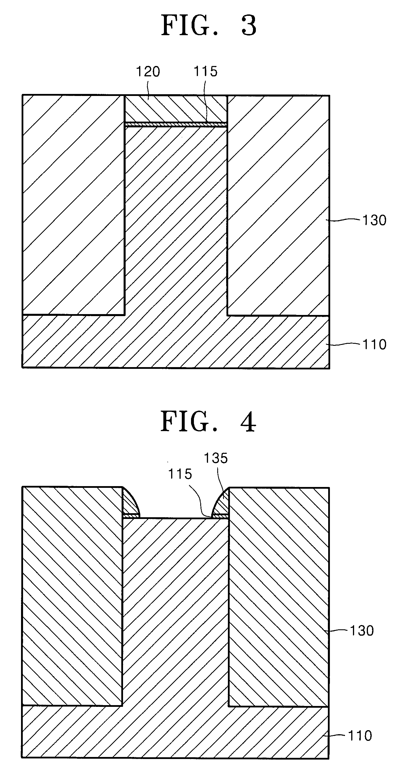
[0016] Example embodiments will now be described more fully with reference to the accompanying drawings. Example embodiments may, however, be embodied in many different forms and should not be construed as being limited to the examples set forth herein. The sizes of elements in the drawings may have been exaggerated for purposes of illustration.
[0017] It will be understood that when an element or layer is referred to as being “on”, “connected to”, “coupled to”, or “covering” another element or layer, it may be directly on, connected to, coupled to, or covering the other element or layer or intervening elements or layers may be present. In contrast, when an element is referred to as being “directly on,”“directly connected to” or “directly coupled to” another element or layer, there are no intervening elements or layers present. Like numbers refer to like elements throughout. As used herein, the term “and / or” includes any and all combinations of one or more of the associated listed i...
PUM
 Abstract
Description
Claims
Application Information