Semiconductor device

a memory device and semiconductor technology, applied in the field of semiconductor memory devices, can solve the problems of high integration difficulty, high wiring operation difficulty, and extremely difficult to achieve, and achieve the effects of reducing power consumption, improving integration degree, and high-precision writing operation

Inactive Publication Date: 2014-04-01
SEMICON ENERGY LAB CO LTD
View PDF31 Cites 10 Cited by
  • Summary
  • Abstract
  • Description
  • Claims
  • Application Information

AI Technical Summary

Benefits of technology

[0013]In view of the above problems, an object of one embodiment of the disclosed invention is to provide a semiconductor memory device which is capable of shortening a time needed for holding desired charges in all memory cells on one word line by determining the potentials of the memory cells on the word line concurrently. Further, an object of one embodiment of the disclosed invention is to provide a semiconductor memory device whose power consumption is reduced and whose reliability is improved by improving an integration degree and achieving highly precise writing operation and highly precise reading operation. Further, an object of one embodiment of the disclosed invention is to provide a semiconductor memory device having a novel feature, in which a transistor including an oxide semiconductor (a transistor having high holding characteristics and favorable switching characteristics) is provided.
[0024]According to one embodiment of the disclosed invention, by concurrently determining the potentials of the memory cells on one word line, the semiconductor memory device in which a time needed for holding the desired charges in all of the memory cells on the one word line can be shortened can be obtained. In addition, the integration degree is improved and high-precision writing operation and high-precision reading operation can be achieved, whereby power consumption can be reduced and the semiconductor memory device with improved reliability can be obtained. In addition, the semiconductor memory device having a novel feature provided with a transistor including an oxide semiconductor can be obtained.

Problems solved by technology

As described above, in a NOR type semiconductor memory device, the potentials of the memory cells on one word line cannot be determined concurrently, which is one factor of hindering high speed wiring operation.
A multi-valued NOR type semiconductor memory device in which threshold voltages are set at multiple levels has a problem of difficulty in high integration because a complicated control circuit is also needed.
Consequently, appropriate control of a threshold voltage window width, highly precise writing operation, and highly precise reading operation are needed, but it is extremely difficult to achieve them.

Method used


Image

  • Semiconductor device
  • Semiconductor device
  • Semiconductor device

Examples


embodiment 1

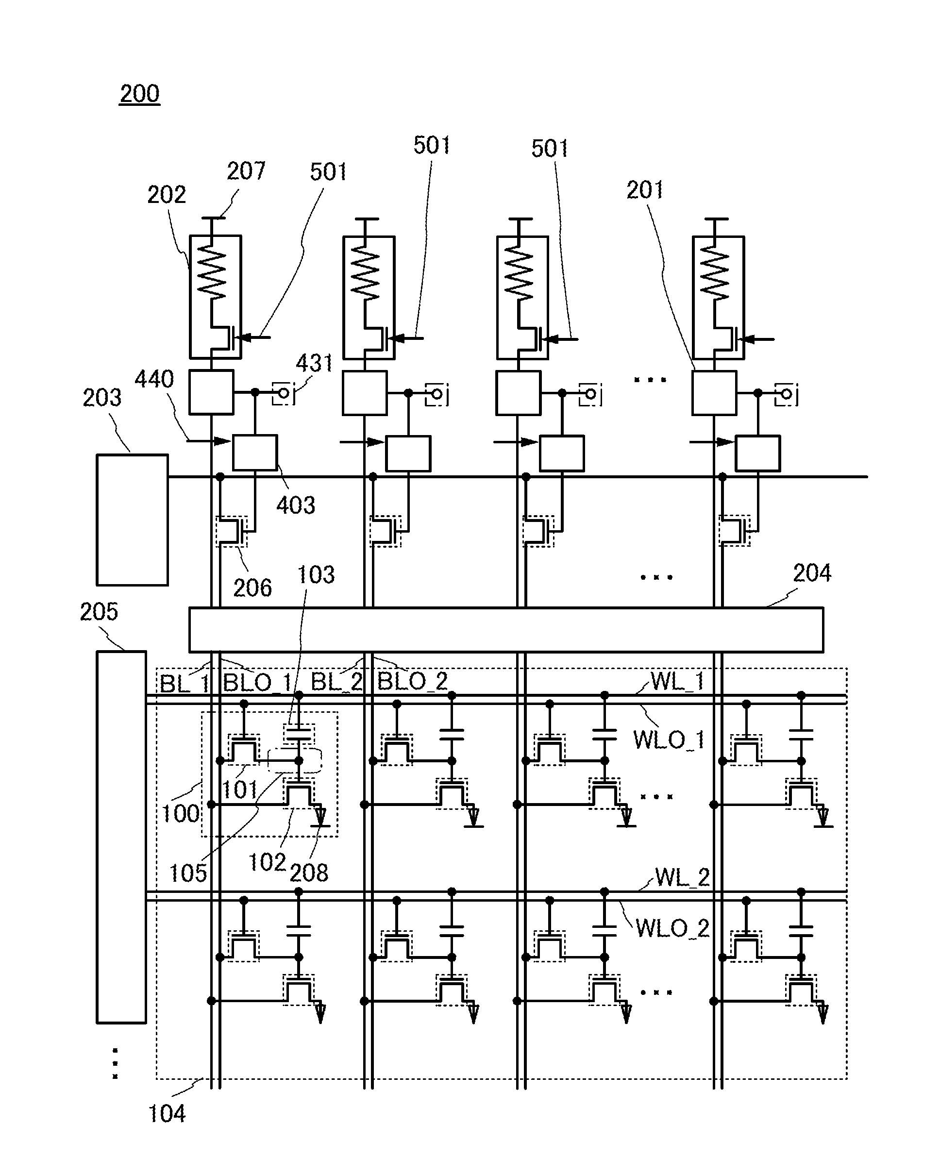
[0035]In this embodiment, a circuit configuration and a method for driving a semiconductor memory device according to one embodiment of the disclosed invention will be described with reference to FIG. 1, FIG. 2, FIGS. 3A and 3B, and FIGS. 4A and 4B. Note that the method for driving the semiconductor memory device according to one embodiment of the disclosed invention allows concurrent determination of potentials of memory cells on one word line.

[0036]First, an example of a circuit configuration of a semiconductor memory device according to one embodiment of the disclosed invention is described with reference to FIG. 1. Note that in FIG. 1, all components of the semiconductor memory device are not illustrated, and a device which cannot be illustrated, a complicated peripheral circuit, and the like are omitted.

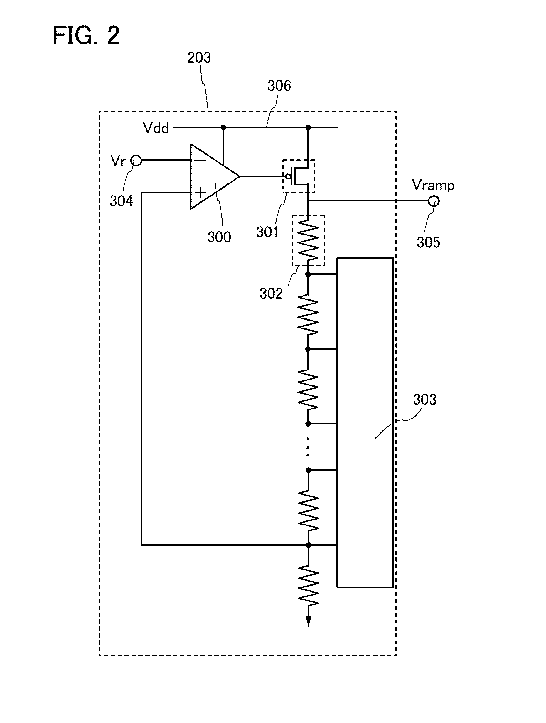
[0037]A semiconductor memory device 200 illustrated in FIG. 1 includes a plurality of reading circuits 201, a plurality of control circuits 202, a potential control circuit 203,...


PUM


Abstract

An object is to provide a semiconductor memory device capable of shortening writing operation by concurrently determining potentials of memory cells on one word line. A plurality of transistors having switching characteristics are connected to one potential control circuit, whereby writing potentials are determined concurrently. A potential continues to be changed (raised or decreased) stepwise, a desired potential is determined while changing the potential, and whether data resulted from reading with respect to written data is correct or not is continuously checked, so that high-precision writing operation and high-precision reading operation can be achieved. In addition, favorable switching characteristics and holding characteristics of a transistor including an oxide semiconductor are utilized.

Description

BACKGROUND OF THE INVENTION[0001]1. Field of the Invention[0002]The invention disclosed herein relates to a semiconductor memory device using a semiconductor element and a method for driving the semiconductor memory device.[0003]2. Description of the Related Art[0004]At present, a dominating non-volatile ROM is a batch-erasing-type memory referred to as a flash memory. A flash memory is largely divided into a NOR type flash memory and a NAND type flash memory. A NOR type flash memory is used for firmware, a BIOS, and program code storage of an electronic appliance such as a mobile phone. A NAND type flash memory is used for a large capacity memory and an SD card.[0005]Although a NOR type memory device has high reliability, an increase in speed at the time of writing, an improvement in power consumption, an improvement in integration degree, and the like are issues of a NOR type memory device. Although a NAND type memory device can have a high integration degree and large capacity, a...

Claims


Application Information

Patent Timeline
Patent Type & Authority Patents(United States)
IPC IPC(8): H01L29/10
CPCG11C16/0433G11C11/5621G11C16/3404G11C7/10G11C11/34
Inventor KAMATA, KOICHIRO
Owner SEMICON ENERGY LAB CO LTD
Why Eureka
Try Eureka