Semiconductor light emitting device

Active Publication Date: 2008-05-22
NICHIA CORP
View PDF7 Cites 76 Cited by
  • Summary
  • Abstract
  • Description
  • Claims
  • Application Information

AI Technical Summary

Benefits of technology

[0026]According to the semiconductor light emitting device of the third aspect of the present invention, heat that is generated by the semiconductor light emitting element is less likely to be conducted to the cap or the wavelength conversion material. Therefore, it is possible to prevent deterioration of the characteristics of the wavelength conversion material.
[0027]According to the semiconductor light emitting device of the fourth aspect of the present invention, it is possible to reduce return light that returns to the semiconductor light emitting element, that is, to provide a light guide that allows light to pass only in one direction.
[0028]In the semiconductor light emitting device of the fifth aspect of the present invention, since the inclination angle of the wall surface of the penetrating opening is constant, it is easy to form the penetrating opening.
[0029]According to the semiconductor light emitting device of the sixth, eight

Problems solved by technology

In semiconductor light emitting devices, it has been an important issue to allow light to efficiently outgo from a semiconductor light emitting element as a light source.
However, in the thus-configured light emitting device, there is a problem in that a part of ligh

Method used


Image

  • Semiconductor light emitting device
  • Semiconductor light emitting device
  • Semiconductor light emitting device

Examples


first embodiment

Configuration

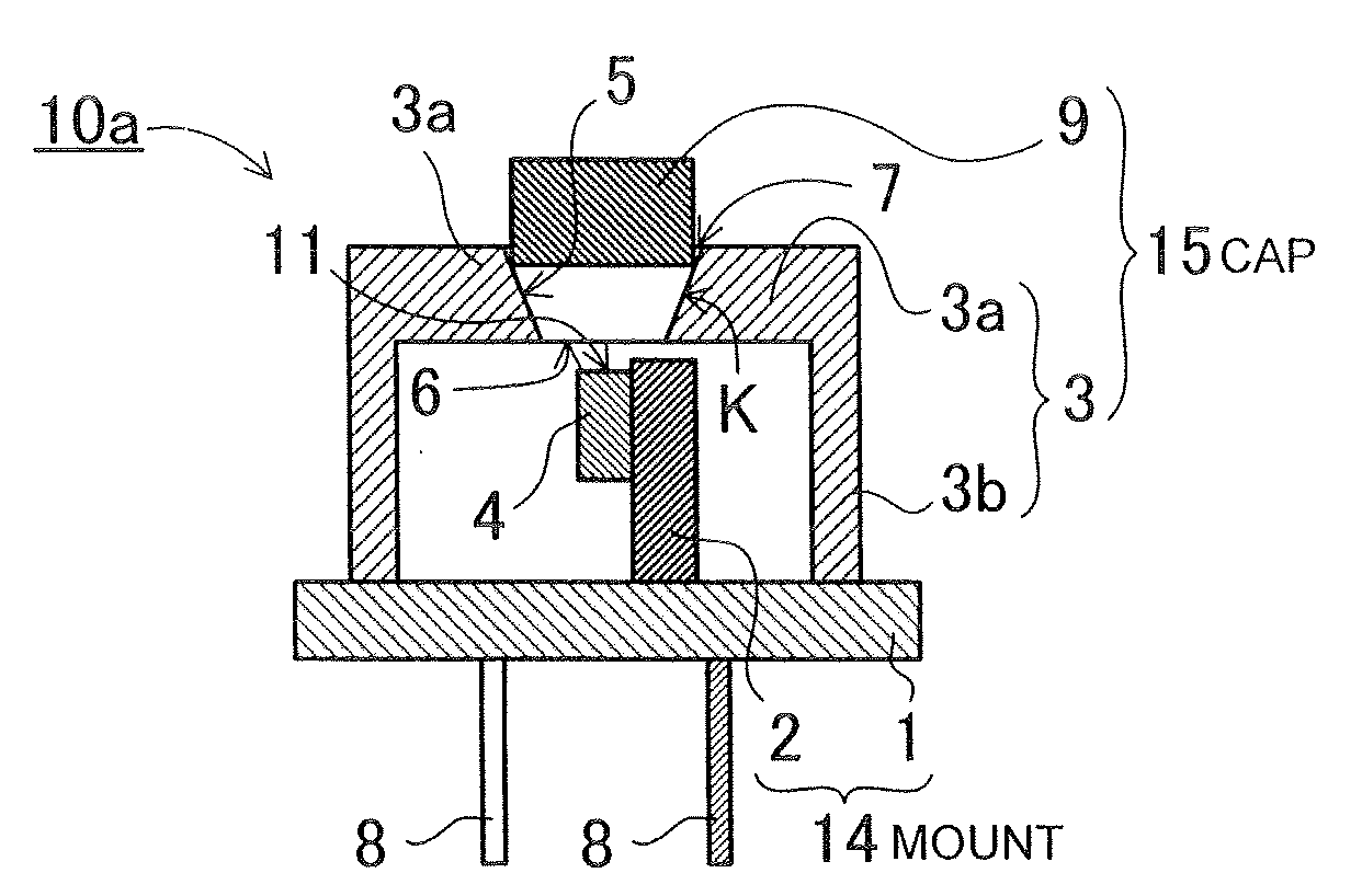
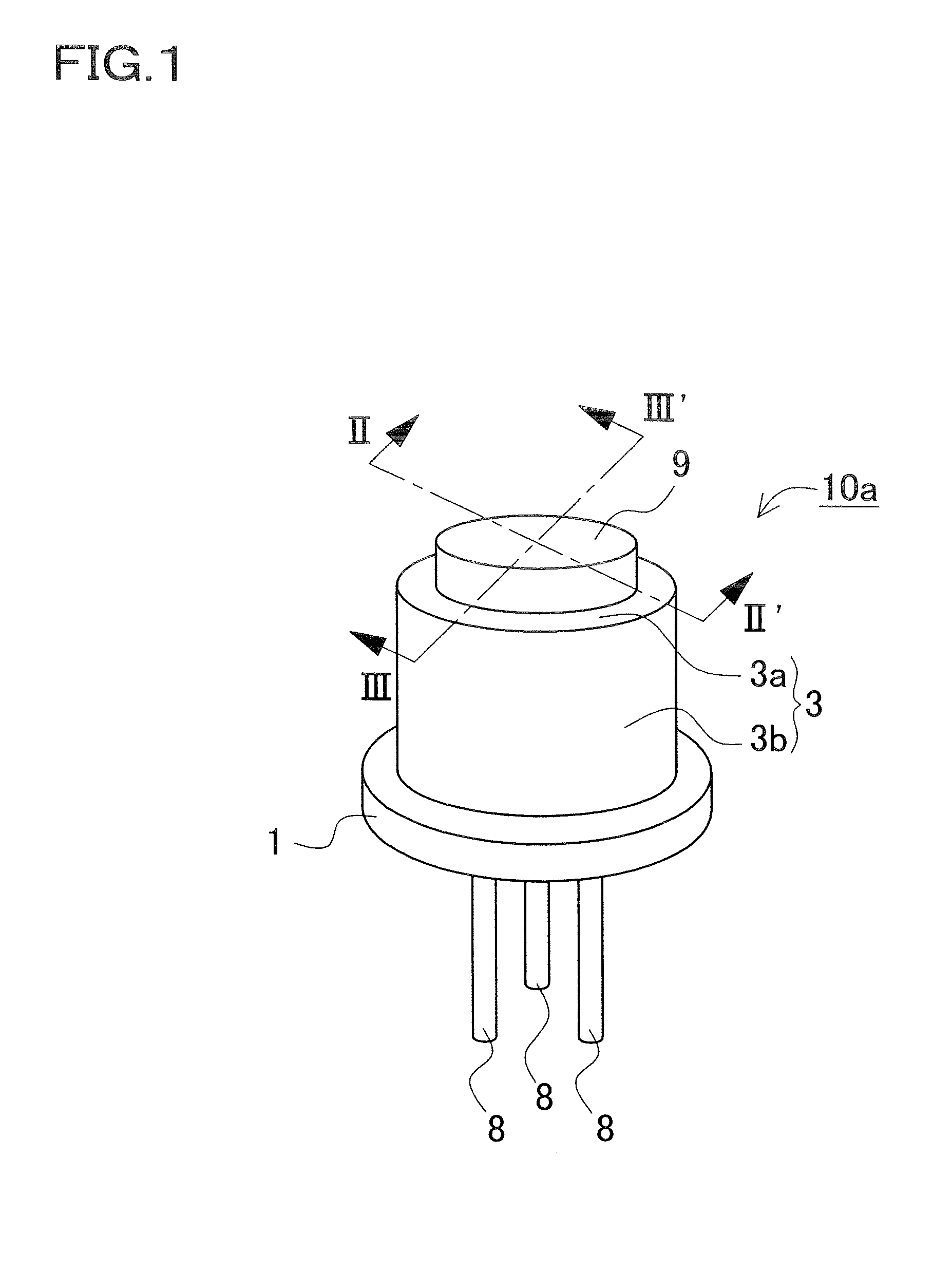
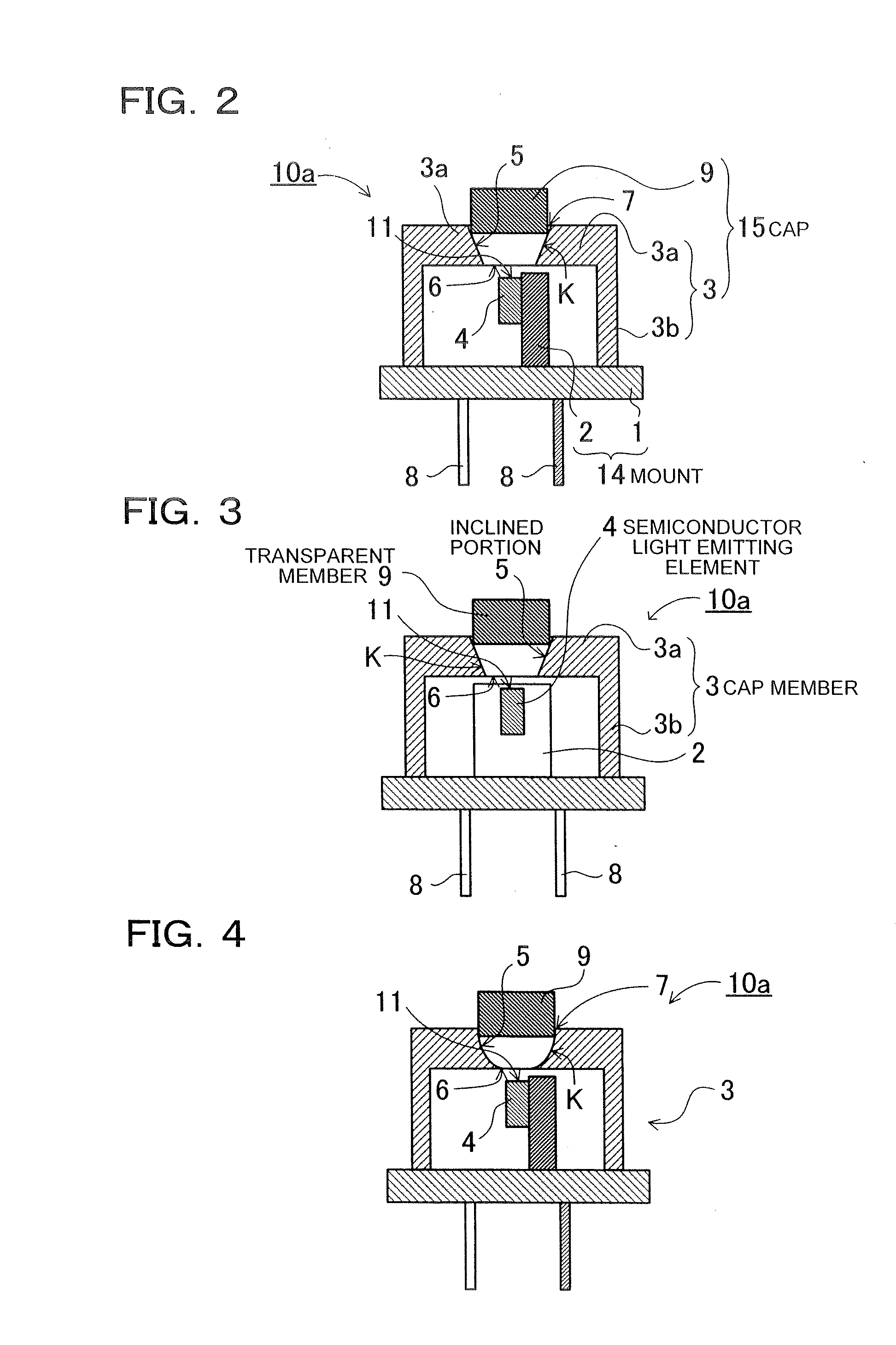
[0059]FIG. 1 is a perspective view showing a semiconductor light emitting device 10a according to a first embodiment. FIG. 2 is a cross-sectional view of the semiconductor light emitting device 10a shown in FIG. 1 taken along the line II-II′. FIG. 3 is a cross-sectional view of the semiconductor light emitting device 10a shown in FIG. 1 taken along the line III-III′. In the semiconductor light emitting device 10a, as shown in FIG. 1, leads 8 extend in the vertical direction from the bottom surface (lower surface in FIG. 1) of the disk-shaped stem base 1. The leads 8 can be electrically connected to external terminals. A cylindrical cap member 3 is adhered onto the upper surface (upper surface in FIG. 1) of the stem base 1 in proximity to the periphery of the stem base 1 so that the center axis of the cylindrical cap member 3 extends in the vertical direction. The cap member 3 has an annular upper surface 3a that is coupled to the upper rim of a side surface 3b of the ca...

second embodiment

[0090]FIG. 6 is a cross-sectional view showing a semiconductor light emitting device 10b according to a second embodiment. The semiconductor light emitting device 10b includes an additional member in addition to the semiconductor light emitting device 10a according to the first embodiment. Accordingly, the same components as those of the foregoing embodiment are attached with numerals with the same reference numerals as those of the foregoing embodiment and their description is omitted.

Cap Cover

[0091]In the semiconductor light emitting device 10b according to the second embodiment, as shown in FIG. 6, a cap cover 16 is additionally mounted outside the cap member 3. The cap cover 16 includes a cylindrical cap cover member 13 that has an opening, and a transparent plate 12 that closes this opening. The cap cover member 13 has a cylindrical side surface 13b and an upper surface 13a that covers the upper part of the side surface 13b. Also, the cap cover member 13 has substantially the s...

third embodiment

[0095]FIG. 7(a) shows a semiconductor light emitting device 10c according to a third embodiment. The semiconductor light emitting device 10c has difference with the semiconductor light emitting device 10a according to the first embodiment in the shape of a transparent member. In other words, the semiconductor light emitting device 10c has configuration similarly to the first embodiment except for the shape of the transparent member. Accordingly, the description of configuration similarly to the first embodiment is omitted.

[0096]As shown in FIG. 7 (a), in the semiconductor light emitting device 10c according to the third embodiment, a transparent member 9b has a substantially inverted truncated cone shape. The inclination angle of the side surface of the transparent member 9b is the same as that of the inclined portion 5. Thus, the transparent member 9b comes in tight contact with the wall surface of the inclined portion 5. The transparent member 9b closes the penetrating opening K f...


PUM


Abstract

A semiconductor light emitting device is provided which allows emission light from a light source to efficiently outgo from the semiconductor light emitting device so that the light emission intensity of the semiconductor light emitting device is increased. A penetrating opening is formed in the substantially central part of a cap member to communicate the interior side to the exterior side the cap member. The penetrating opening has an inclined portion. The inclined portion is opposed to and spaced away from a semiconductor light emitting element and includes a light entering portion through which emission light from the semiconductor light emitting element passes. The opening width of the inclined portion is getting wider from the light entering portion in the light traveling direction so that the inclined portion is tapered. The emission light from the semiconductor light emitting element can effectively outgo from the semiconductor light emitting device.

Description

BACKGROUND OF THE INVENTION[0001]1. Technical Field[0002]The present invention relates to a semiconductor light emitting device that includes a semiconductor light emitting element, and in particular to a semiconductor light emitting device that allows light from a light source to efficiently outgo from the semiconductor light emitting device.[0003]2. Description of Related Art[0004]In semiconductor light emitting devices, it has been an important issue to allow light to efficiently outgo from a semiconductor light emitting element as a light source. Accordingly, various types of light emitting devices have been developed. FIG. 25(a) shows a known LED light emitting device 200 (see Japanese Laid-Open Patent Publication No. H07-099345 (1995)). The LED light emitting device 200 is configured to entirely seal a semiconductor light emitting device with a resin member. The semiconductor light emitting member includes a lead frame 202 that includes a cup 203, and an LED 204 that is mounte...

Claims


Application Information

Patent Timeline
IPC IPC(8): H01L33/00H01L33/48H01L33/50H01L33/58
CPCH01L2224/32257H01L2224/48471H01L2224/49107H01L2224/8592H01L33/483H01L33/505H01L2224/48247H01L33/58H01L2224/48091H01L2224/73265H01L33/507H01L2224/48257H01L2224/32245H01L2924/00014H01L2924/00H01L2924/181H01L2924/00012
Inventor SUGIYAMA, TAKAFUMI
Owner NICHIA CORP
Why Eureka
Try Eureka