

Electronic component, mounting structure of electronic component, and process for producing electronic component
a technology for electronic components and mounting structures, applied in the direction of fixed capacitor details, printed circuit non-printed electric components association, capacitor manufacture, etc., can solve the problems of reducing the resistance of multi-layer ceramic capacitors mounted on mounting objects such as circuit boards, and deteriorating reliability, and achieve the effect of satisfying the solderability of external electrodes
- Summary
- Abstract
- Description
- Claims
- Application Information
AI Technical Summary
Benefits of technology
Problems solved by technology
Method used
Image

Examples
example 1
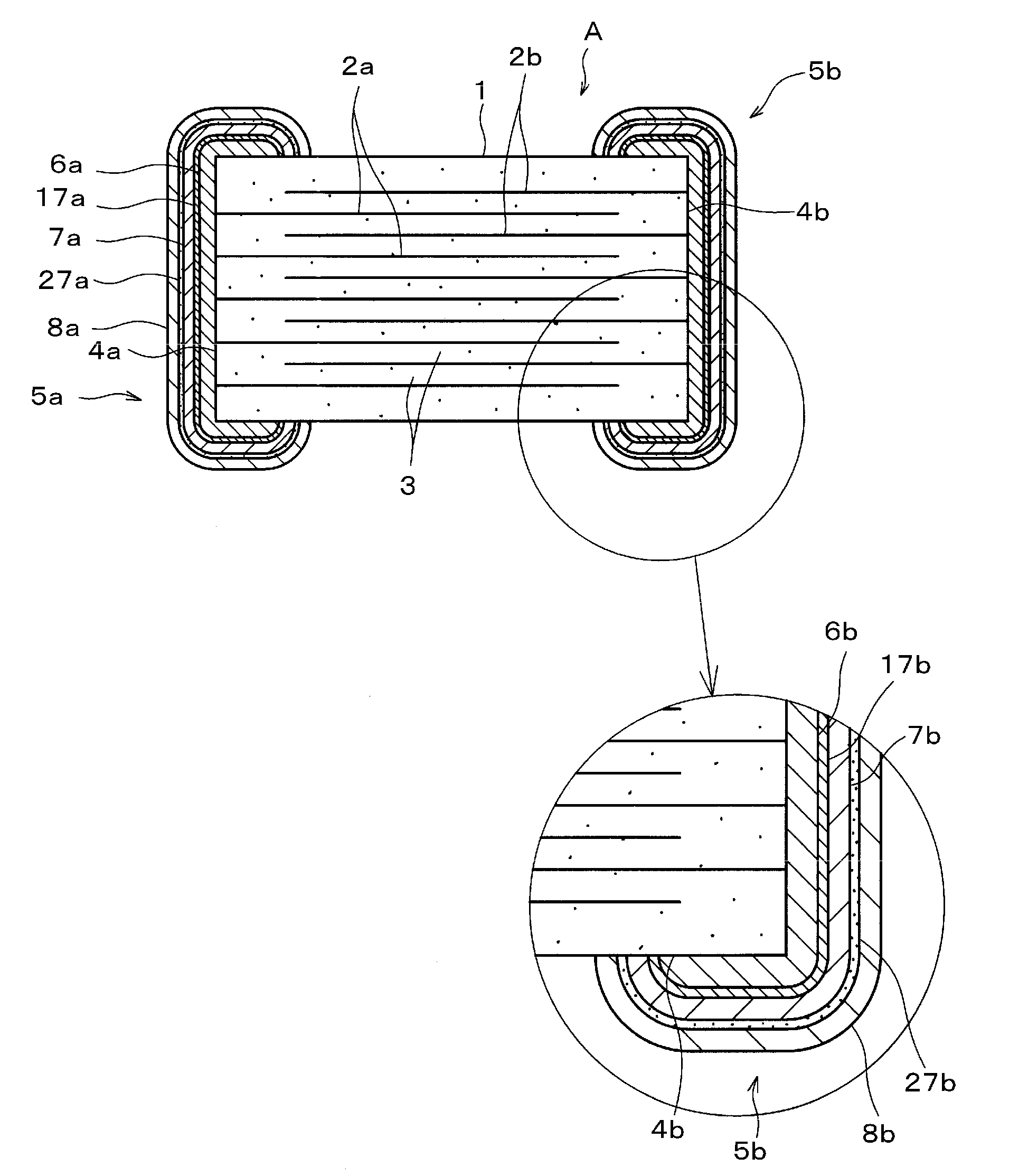
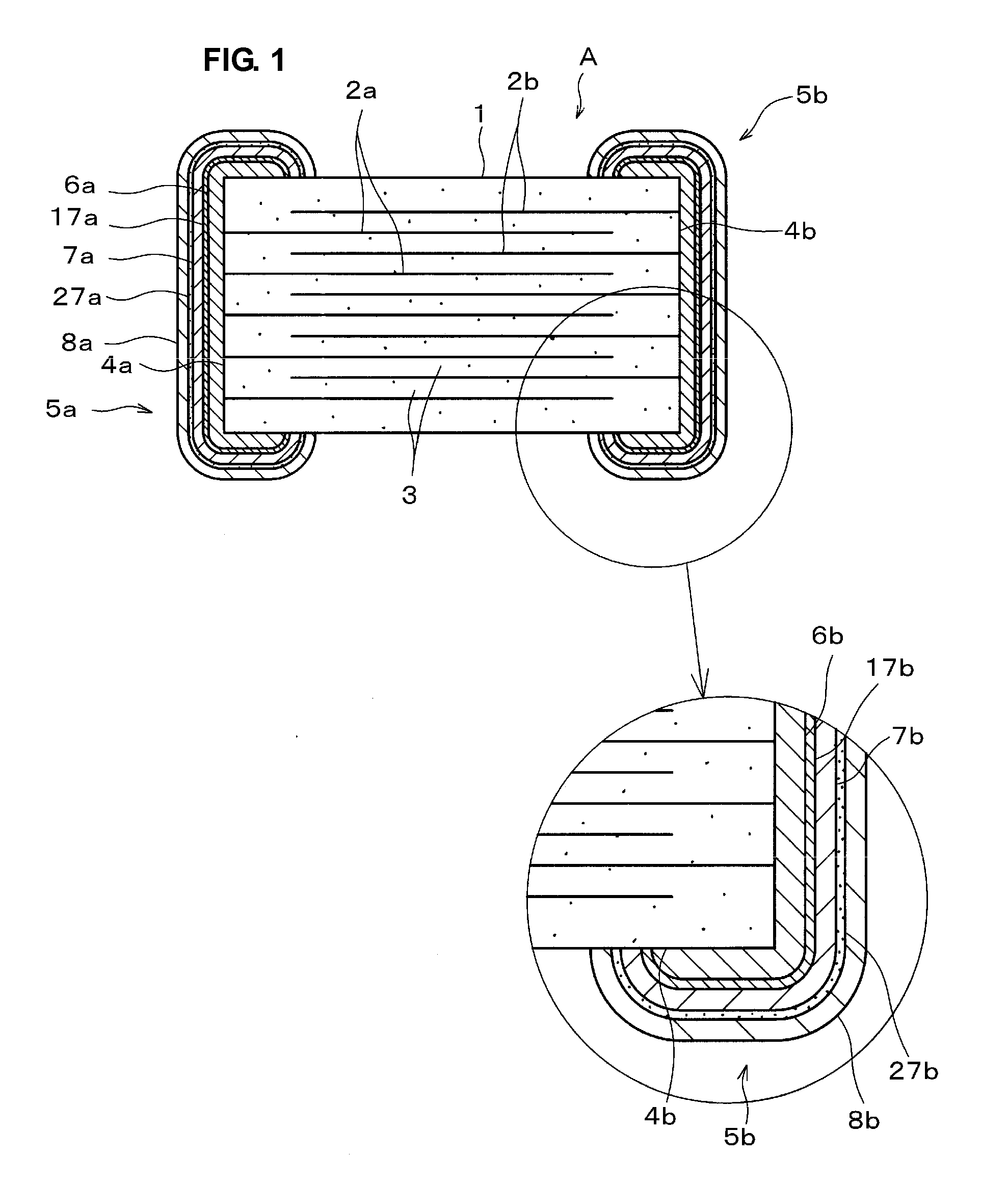
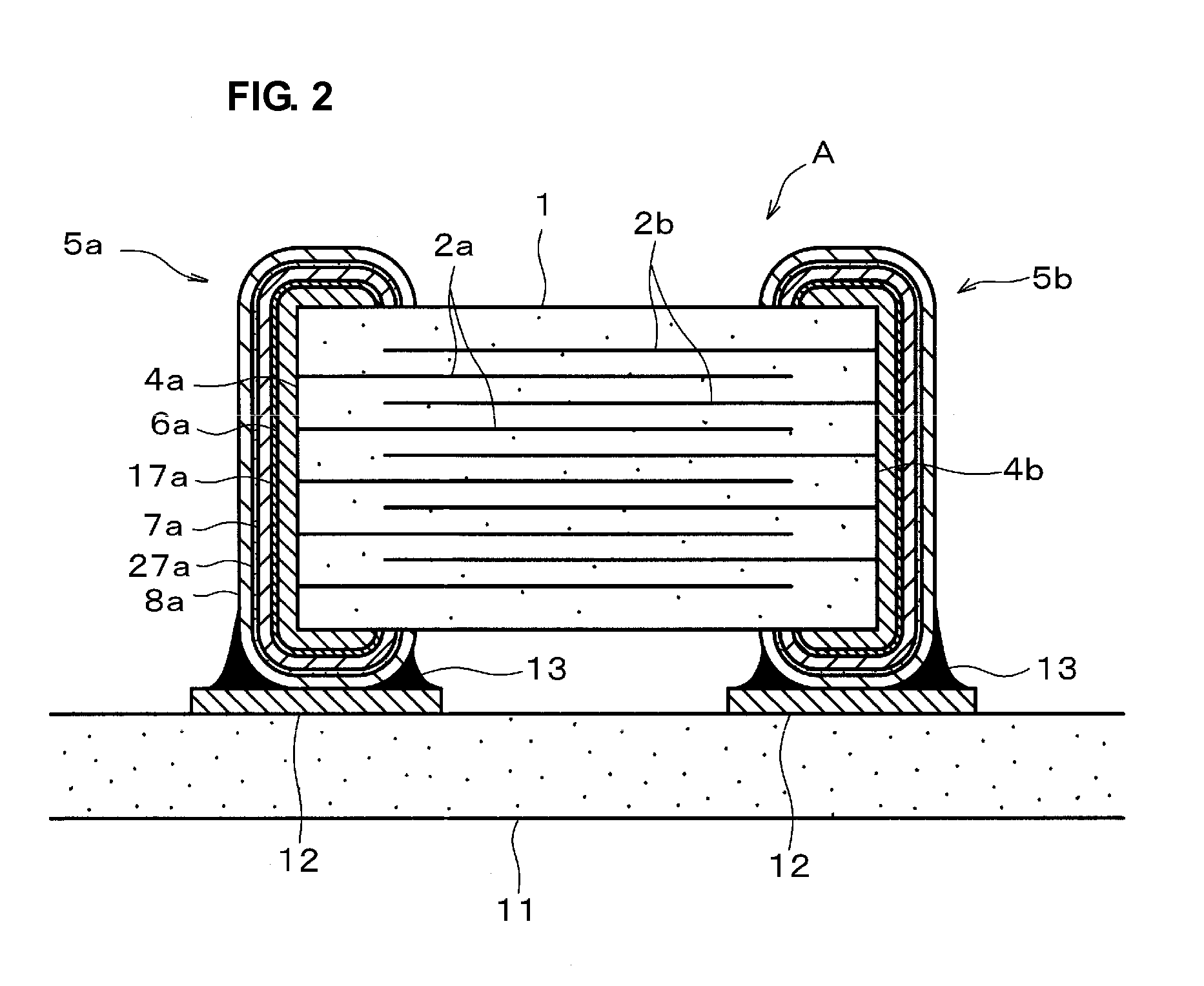
[0046]FIG. 1 is a cross-sectional view of an electronic component (multilayer ceramic capacitor in this EXAMPLE) A produced by a process for producing an electronic component according to an example (EXAMPLE 1) of a preferred embodiment of the present invention.
[0047]As shown in FIG. 1, the multilayer ceramic capacitor A includes a plurality of internal electrodes (Ni electrodes) 2a and 2b alternately disposed; ceramic layers 3, each internal electrode 2a being opposite the corresponding internal electrode 2b with a corresponding one of the ceramic layers 3 provided therebetween; a ceramic body (main body of the electronic component) 1 having end surfaces 4a and 4b, the internal electrodes 2a being connected to the end surface 4a, and the internal electrodes 2b being connected to the end surface 4b; and a pair of external electrodes 5a and 5b, the external electrodes 5a and 5b being disposed on the end surfaces 4a and 4b, respectively, and being connected to the internal electrodes ...
example 2
[0102]In EXAMPLE 2, multilayer ceramic capacitors having the similar structure shown in FIG. 1 as in EXAMPLE 1 were produced in the same production process and the same production conditions as in EXAMPLE 1.
[0103]However, in EXAMPLE 2, conditions for heat-treating the Ni plating layers 7a and 7b disposed on the underlying electrode layers 6a and 6b were as follows. Any other condition was the same as in EXAMPLE 1.[0104](a) Heat-treatment temperature:[0105]300° C., 500° C., 700° C., 900° C., and 1100° C.[0106](b) Oxygen concentration in heat treatment:[0107]50 ppm, 100 ppm, and 150 ppm[0108](c) Heat-treatment time:[0109]1 hour
[0110]The resulting multilayer ceramic capacitors were subjected to reflow soldering with lead-free solder containing Zn at about 230° C. in a N2 atmosphere to be mounted on a board. The multilayer ceramic capacitors were left standing for approximately 144 hours at about 125° C., about 1.2 atm, and about 95% RH while a rated voltage was applied, for example. A ...
example 3
[0121]In EXAMPLE 3, multilayer ceramic capacitors having the similar structure shown in FIG. 1 as in EXAMPLE 1 were produced in the same production process and the same production conditions as in EXAMPLE 1.
[0122]However, in EXAMPLE 3, conditions for heat-treating the Ni plating layers disposed on the underlying electrode layers were as follows. Furthermore, the thickness of each Ni plating layer was changed as follows. Other conditions were identical to those in EXAMPLES 1 and 2.
[0123]Heat-Treatment Condition[0124](a) Heat-treatment temperature:[0125]600° C.[0126](b) Oxygen concentration in heat treatment:[0127]50 ppm[0128](c) Heat-treatment time:[0129]0.5 hour, 1 hour, and 2 hours
Thickness of Ni Plating Layer
[0130]0.5 μm, 1.0 μm, 3.0 μm, 5.0 μm, 7.0 μm, and 9.0 μm
[0131]The resulting multilayer ceramic capacitors were subjected to reflow soldering with lead-free solder containing Zn at about 230° C. in a N2 atmosphere to be mounted on a board. The multilayer ceramic capacitors were...
PUM
| Property | Measurement | Unit |
|---|---|---|
| Temperature | aaaaa | aaaaa |
| Temperature | aaaaa | aaaaa |
| Fraction | aaaaa | aaaaa |
Abstract
Description
Claims
Application Information