Method of programming a NAND flash memory device
- Summary
- Abstract
- Description
- Claims
- Application Information
AI Technical Summary
Benefits of technology
Problems solved by technology
Method used
Image


Examples
Embodiment Construction
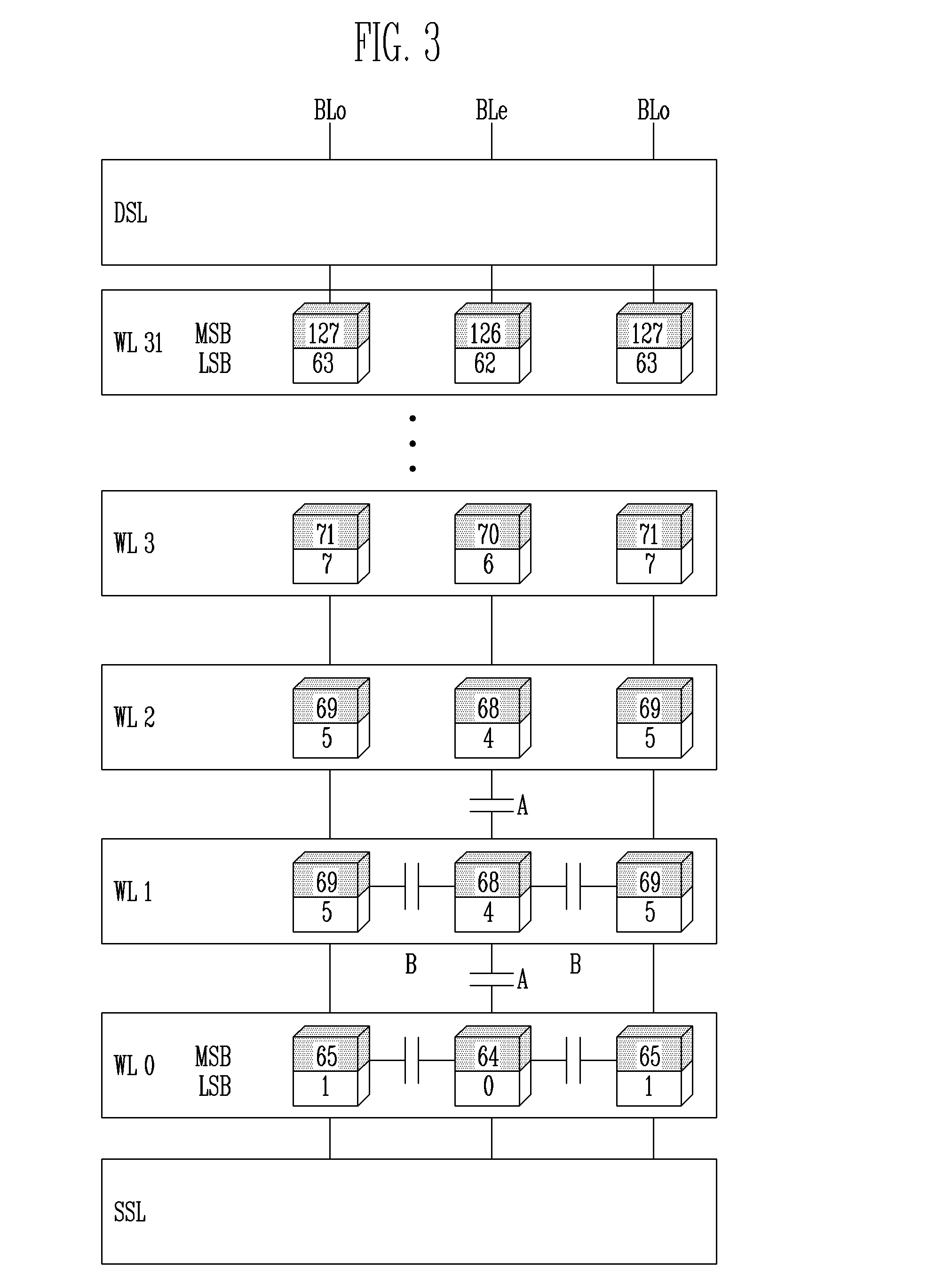
[0030]FIG. 3 is a view illustrating schematically a memory cell array using multi level cell (MLC). A plurality of word lines WL0, WL1 . . . WL31 are formed between a drain selecting line DSL and a source selecting line SSL.
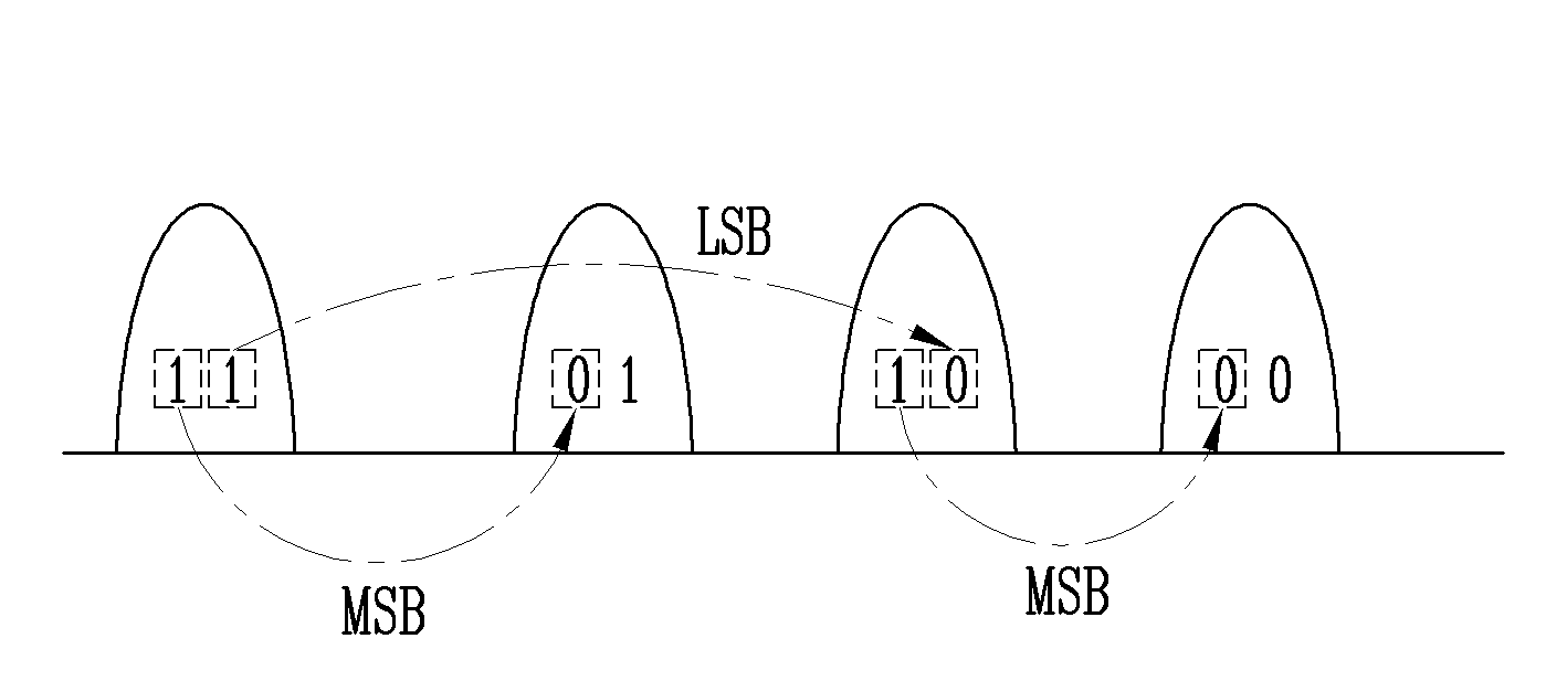
[0031]First, an even LSB program operation (0) is performed to store a lower rank data bit in memory cells coupled to an even bit line BLe that is coupled to the word line WL0 adjacent to the source selecting line SSL.
[0032]Next, an odd LSB program operation (1) is performed to store the lower rank data bit in memory cells coupled to odd bit lines BLo of that is coupled to the word line WL0.
[0033]The even LSB program operation and odd LSB program operation (0 to 63) are repeatedly performed from the word line WL0 to word line WL31. As a result, the lower rank data bits are stored in all of the memory cells coupled to the word lines WL0, WL1 . . . WL31. That is, the even LSB program operation and odd LSB program operation (0 to 63) are performed from the word line...
PUM
 Abstract
Description
Claims
Application Information