

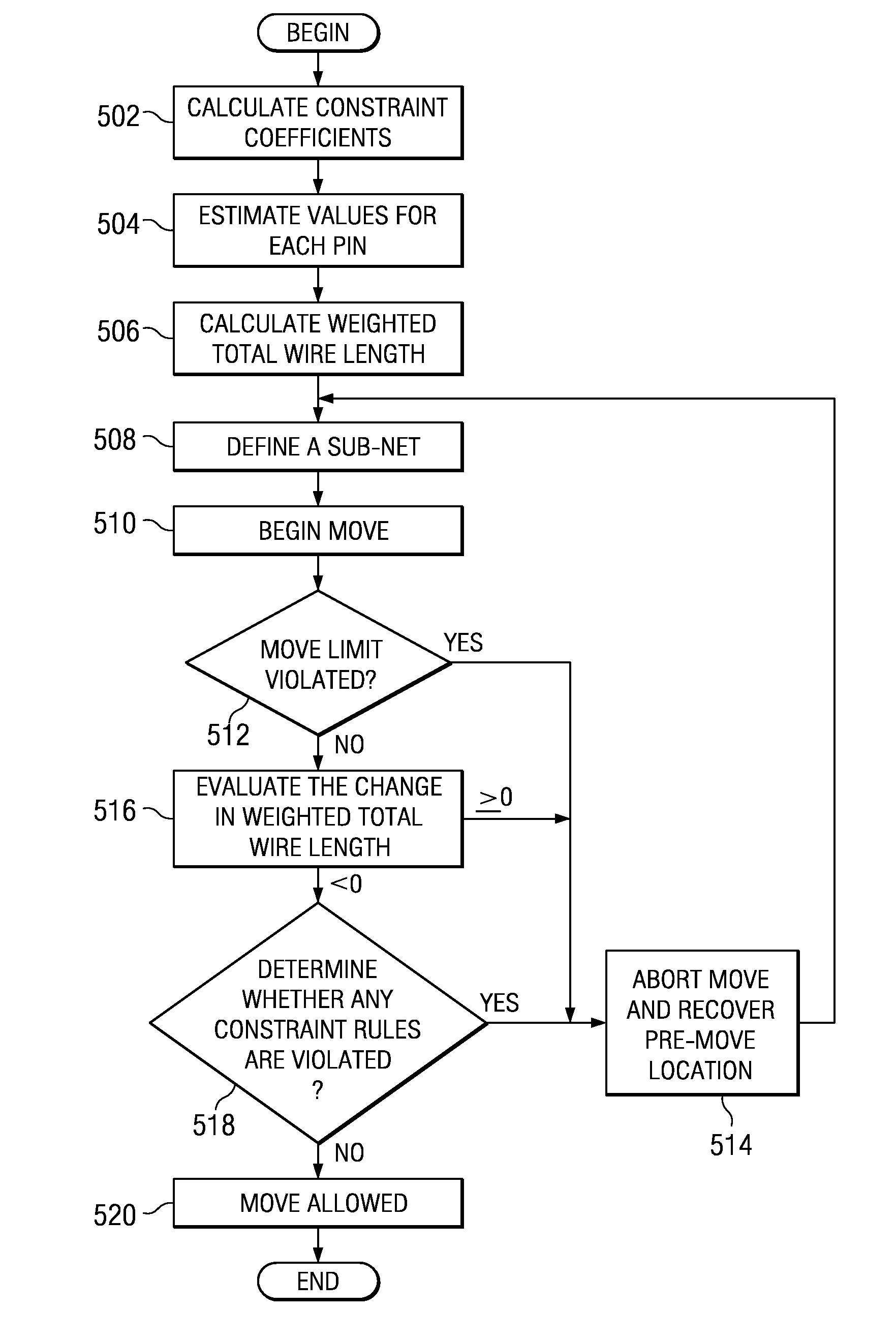
Constrained detailed placement
a detailed placement and constraining technology, applied in the field of data processing systems for physical synthesis of semiconductor devices, can solve the problems of overlap between cells, degradation of wire length, and insufficient optimization, and achieve the effect of reducing the overall length of wires
- Summary
- Abstract
- Description
- Claims
- Application Information
AI Technical Summary
Problems solved by technology
Method used
Image

Examples
Embodiment Construction
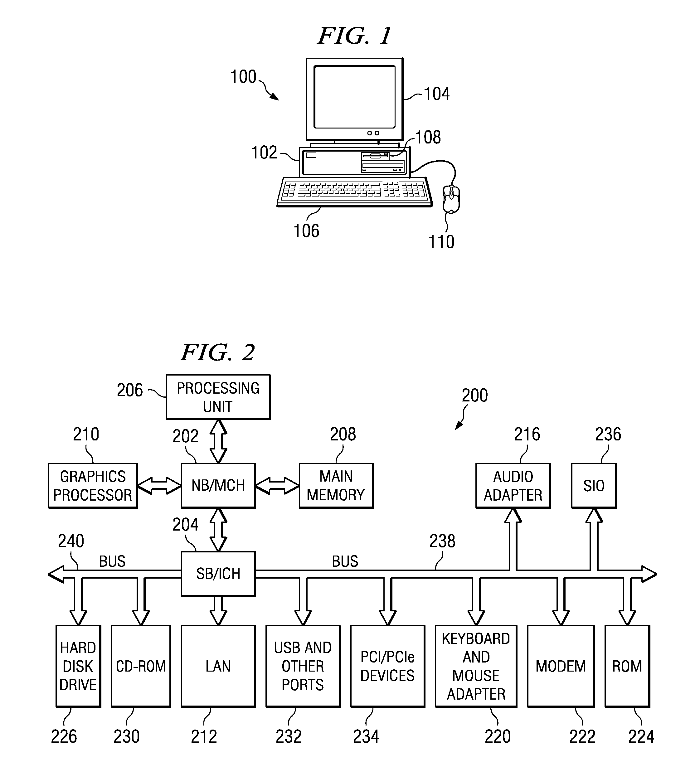
[0016]With reference now to the figures and in particular with reference to FIG. 1, a pictorial representation of a data processing system is shown in which illustrative embodiments may be implemented. Computer 100 includes system unit 102, video display terminal 104, keyboard 106, storage devices 108, which may include floppy drives and other types of permanent and removable storage media, and mouse 110. Additional input devices may be included with personal computer 100. Examples of additional input devices include a joystick, touchpad, touch screen, trackball, microphone, and the like.
[0017]Computer 100 may be any suitable computer, such as an IBM® eServer™ computer or IntelliStation® computer, which are products of International Business Machines Corporation, located in Armonk, N.Y. Although the depicted representation shows a personal computer, other embodiments may be implemented in other types of data processing systems. For example, other embodiments may be implemented in a ...
PUM
 Abstract
Description
Claims
Application Information