Micro-electro-mechanical systems device and integrated circuit device integrated in a three-dimensional semiconductor structure

a technology of integrated circuit and semiconductor structure, which is applied in the direction of microstructural devices, microstructural technology, basic electric elements, etc., can solve the problems of affecting the performance of the cmos device, the device that does not deliver the required performance of the integrated mems/cmos device, and the current co-integration techniques aimed at producing the integrated device are inadequa

Inactive Publication Date: 2008-06-05
FREESCALE SEMICON INC
View PDF16 Cites 70 Cited by
  • Summary
  • Abstract
  • Description
  • Claims
  • Application Information

AI Technical Summary

Problems solved by technology

However, current co-integration techniques aimed at producing an integrated device are inadequate for a variety of reasons.
First, MEMS-on-top-of-CMOS co-integration requires low temperature MEMS processing, which is not optimal and results in device that does not deliver the required performance for an integrated MEMS/CMOS device.
Second, MEMS-CMOS co-integration requ...

Method used


Image

  • Micro-electro-mechanical systems device and integrated circuit device integrated in a three-dimensional semiconductor structure
  • Micro-electro-mechanical systems device and integrated circuit device integrated in a three-dimensional semiconductor structure
  • Micro-electro-mechanical systems device and integrated circuit device integrated in a three-dimensional semiconductor structure

Examples


Embodiment Construction

[0011]The following detailed description is merely exemplary in nature and is not intended to limit the various embodiments or the application and uses of the various embodiments disclosed below. Furthermore, there is no intention to be bound by any theory presented in the preceding background or the following detailed description.

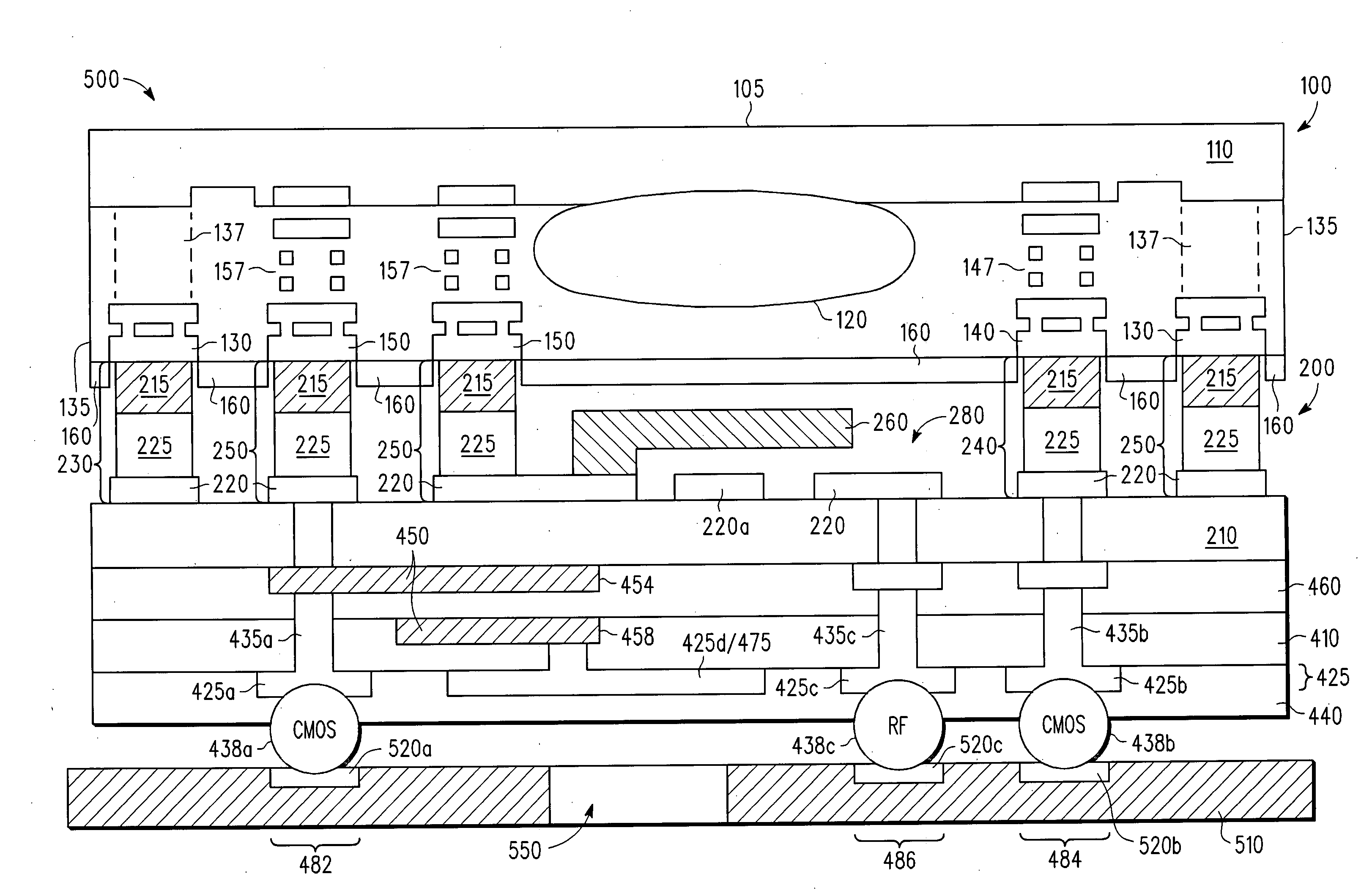
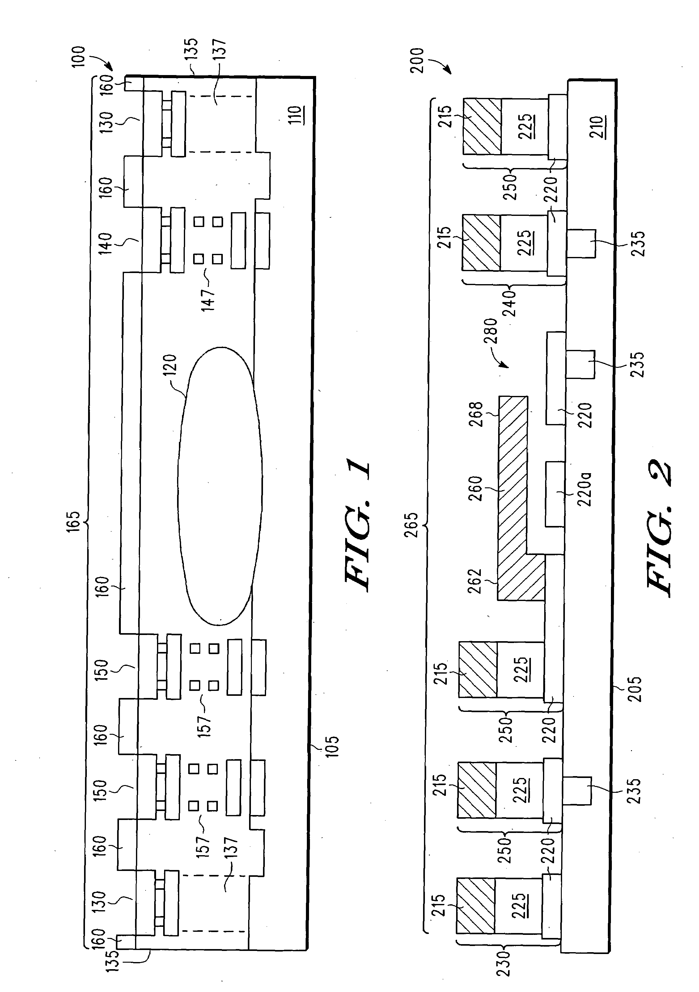
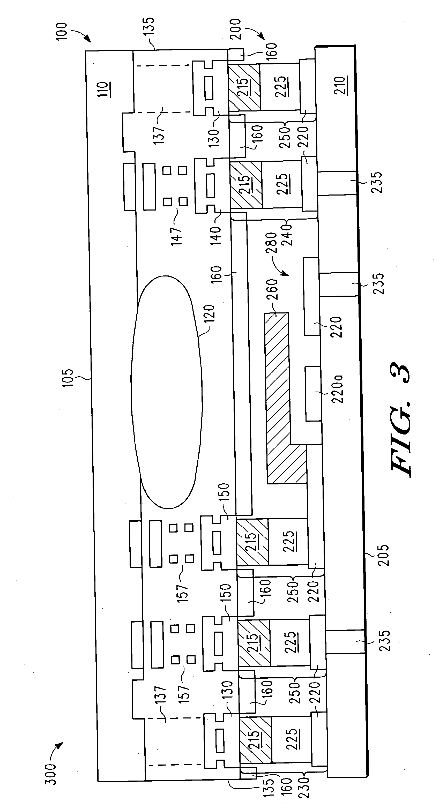
[0012]FIG. 1 is a diagram illustrating one embodiment of an integrated circuit (IC) device 100 including a substrate 110 that forms a back side 105 of IC device 100, wherein substrate 110 may be either a p-type or an n-type substrate. Substrate 110 may be any material known in the art or developed in the future upon which a semiconductor device may be fabricated. Furthermore, substrate 110 may be comprised of any suitable material known in the art or developed in the future for manufacturing semiconductor devices including, for example, a ceramic, a glass, and a semiconductor (e.g., Si, Ge, GaAs, and the like). Moreover, in one embodiment, substrate 110 is...


PUM


Abstract

Semiconductor devices (300, 400, and 500) including an integrated circuit (IC) device (100) coupled to a micro-electro-mechanical systems (MEMS) device (200) and a method (600) for producing same are disclosed. The IC device includes a die seal ring (130) and the MEMS device includes a MEMS seal ring (230), and the IC device is coupled to the MEMS device via the die seal ring and the MEMS seal ring. The MEMS device may include one or more passive devices (450, 475) coupled to it. Moreover, a substrate (510) including an aperture (550) may be coupled to the passive device, wherein the aperture enables the passive device to be trimmed after being disposed on the MEMS device. The semiconductor devices include an RF signal path (486) and at least one other signal path (482 and 484), wherein the other signal path(s) may be an analog and/or a digital signal path.

Description

FIELD OF THE INVENTION[0001]The present invention generally relates to semiconductor devices, and more particularly relates to a micro-electro-mechanical systems (MEMS) device and integrated circuit (IC) device three-dimensionally integrated to form a semiconductor system in module form.BACKGROUND OF THE INVENTION[0002]Reducing the size and cost of semiconductor devices has been one focus of semiconductor research for many years. The desirability of integrating MEMS devices and IC devices is known in the art. However, current co-integration techniques aimed at producing an integrated device are inadequate for a variety of reasons. First, MEMS-on-top-of-CMOS co-integration requires low temperature MEMS processing, which is not optimal and results in device that does not deliver the required performance for an integrated MEMS / CMOS device. Second, MEMS-CMOS co-integration requires changes to the CMOS formation process to accommodate the MEMS formation process, which affects the perform...

Claims


Application Information

Patent Timeline
IPC IPC(8): H01L23/538H01L21/50H01L23/64
CPCB81C1/00238H01L23/585H01L25/16H01L2924/09701H01L2924/0002H01L2924/00
Inventor ZURCHER, PETERD'ACOSTA, CARL E.REMMEL, THOMAS P.
Owner FREESCALE SEMICON INC
Why Eureka
Try Eureka