Organic light-emitting apparatus

US20080150421A1Inactive Publication Date: 2008-06-26CANON KK
18 Cites 36 Cited by

Patent Information

Authority / Receiving Office
US · United States
Current Assignee / Owner
Publication Date
2008-06-26
Estimated Expiration
Not applicable · inactive patent

Smart Images

  • Figure 1
    Figure 1
  • Figure 2
    Figure 2
  • Figure 3
    Figure 3
Patent Text Reader

Abstract

An organic light-emitting apparatus is provided which is reduced in reflection of light incident on an organic light-emitting device and has a high contrast in a light environment. The organic light-emitting apparatus has a number of organic light-emitting devices and has contact holes formed for providing electrical connection to the organic light-emitting devices having a polarizing plate on a light extraction surface side. The organic light-emitting apparatus further has, on the contact holes, an insulating layer which is a light transmissive member, has an opening defining a light-emitting region of the organic light-emitting device, and covers an opening of a planarizing layer and a region between adjacent portions of a first electrodes, and a light shielding layer formed on the insulating layer so as to cover the opening in the planarizing layer.
Need to check novelty before this filing date? Find Prior Art

Description

BACKGROUND OF THE INVENTION

[0001] 2. Field of the Invention

[0002] The present invention relates to an organic light-emitting apparatus provided with an organic electroluminescence (hereinafter, simply referred to as “EL”) device.

[0003] 2. Description of the Related Art

[0004] An organic light-emitting apparatus with a plurality of organic EL devices as organic light-emitting devices designed for being driven by an active matrix circuit has a configuration, for instance, such as illustrated in FIGS. 3 and 4.

[0005] On a glass substrate 500, a thin-film transistor (TFT) 501 is formed which drives an organic light-emitting device (pixel). The TFT 501 has a source region 510, poly-Si 511, a drain region 512, a gate insulating film 513, a gate electrode 514, an interlayer insulating film 515 and a drain electrode 516.

[0006] On the TFT 501, an inorganic insulating film 517 is formed, and an organic planarizing film 518 is further formed thereon so as to level the surface of the inorganic insulati...

Examples

first embodiment

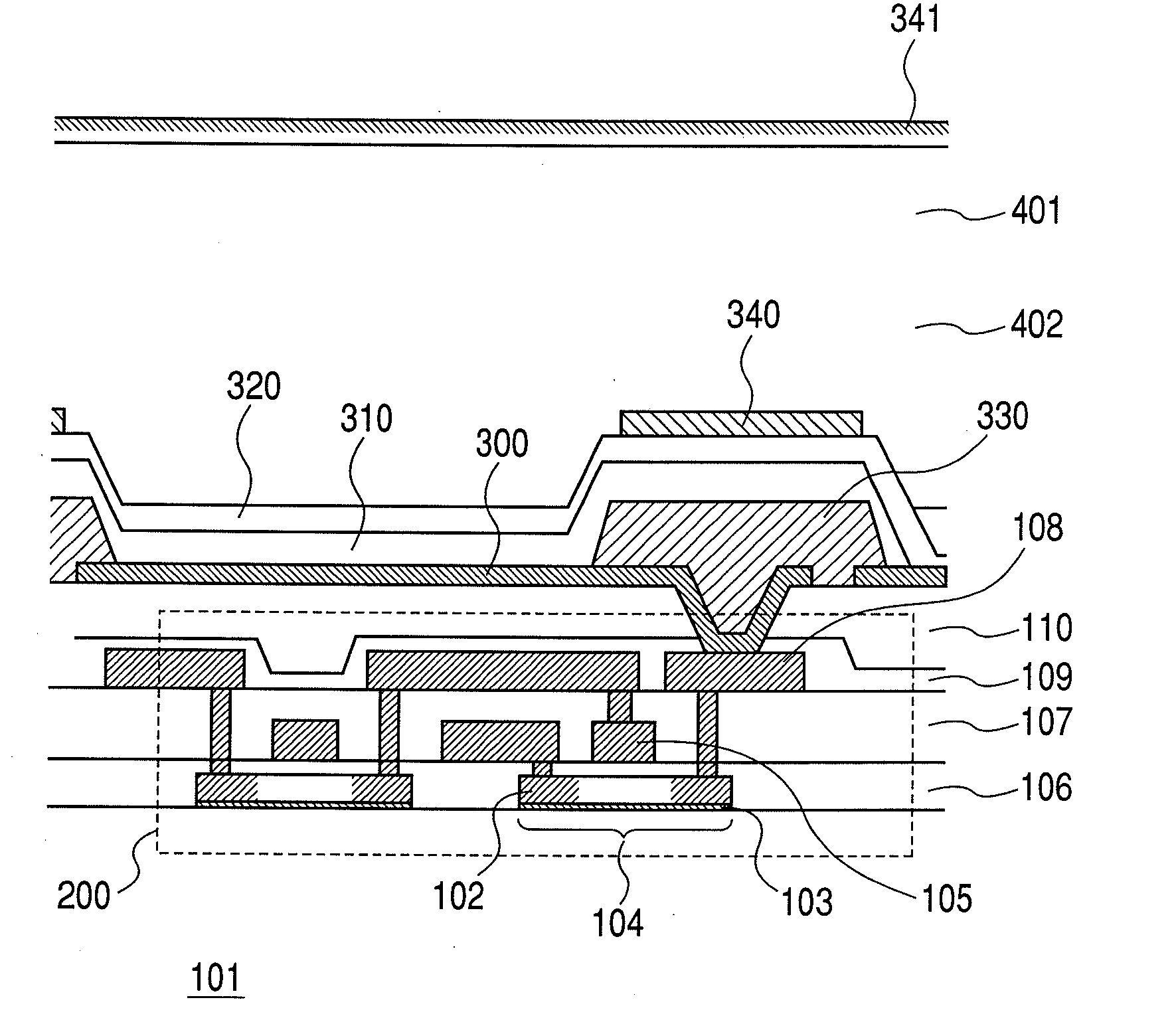
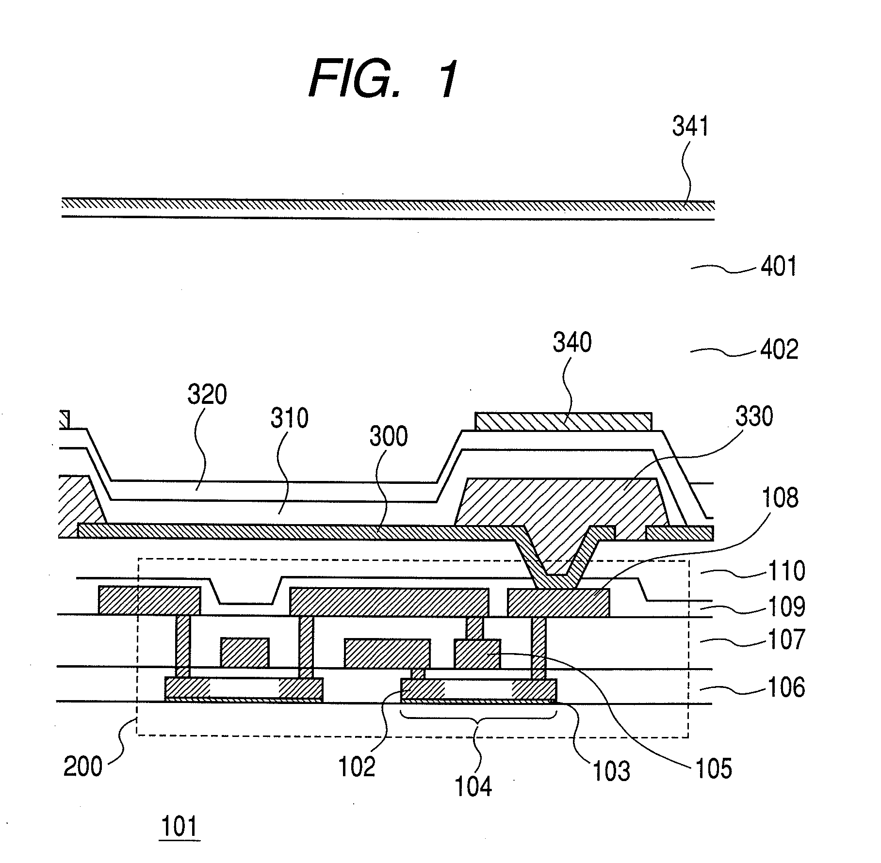
[0048]FIG. 1 is a schematic view illustrating an organic light-emitting apparatus according to the present embodiment.

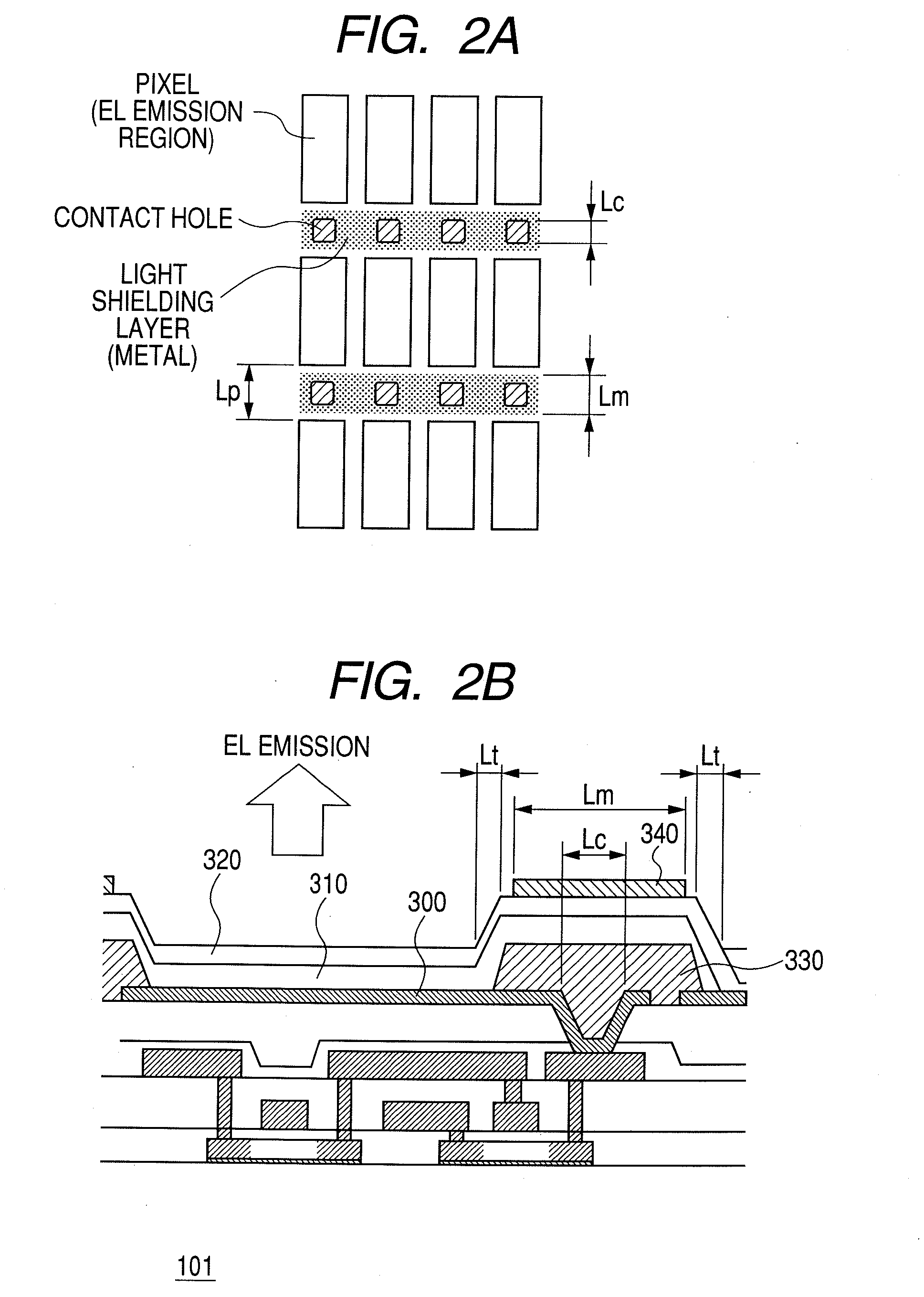
[0049]The organic light-emitting apparatus has a configuration including a plurality of organic light-emitting devices and a polarizing member (polarizing plate) 341 on a light extraction surface side. In addition, an opening (contact hole) is formed between the adjacent organic light-emitting devices, that is, outside a light-emitting region, in order to connect a first electrode (reflective electrode) 300 of the organic light-emitting device and a TFT 200 for driving the organic light-emitting device to each other. On the opening, an insulating layer (device separation layer) 330 made of a resin is formed as a layer for covering the opening. The insulating layer 330 has another opening which is different from the above-mentioned opening (contact hole) and defines a light-emitting region. Further, because the insulating layer 330 is a light transmissive member inclu...