

Circuit board with improved ground plane
- Summary
- Abstract
- Description
- Claims
- Application Information
AI Technical Summary
Benefits of technology
Problems solved by technology
Method used
Image

Examples
first embodiment
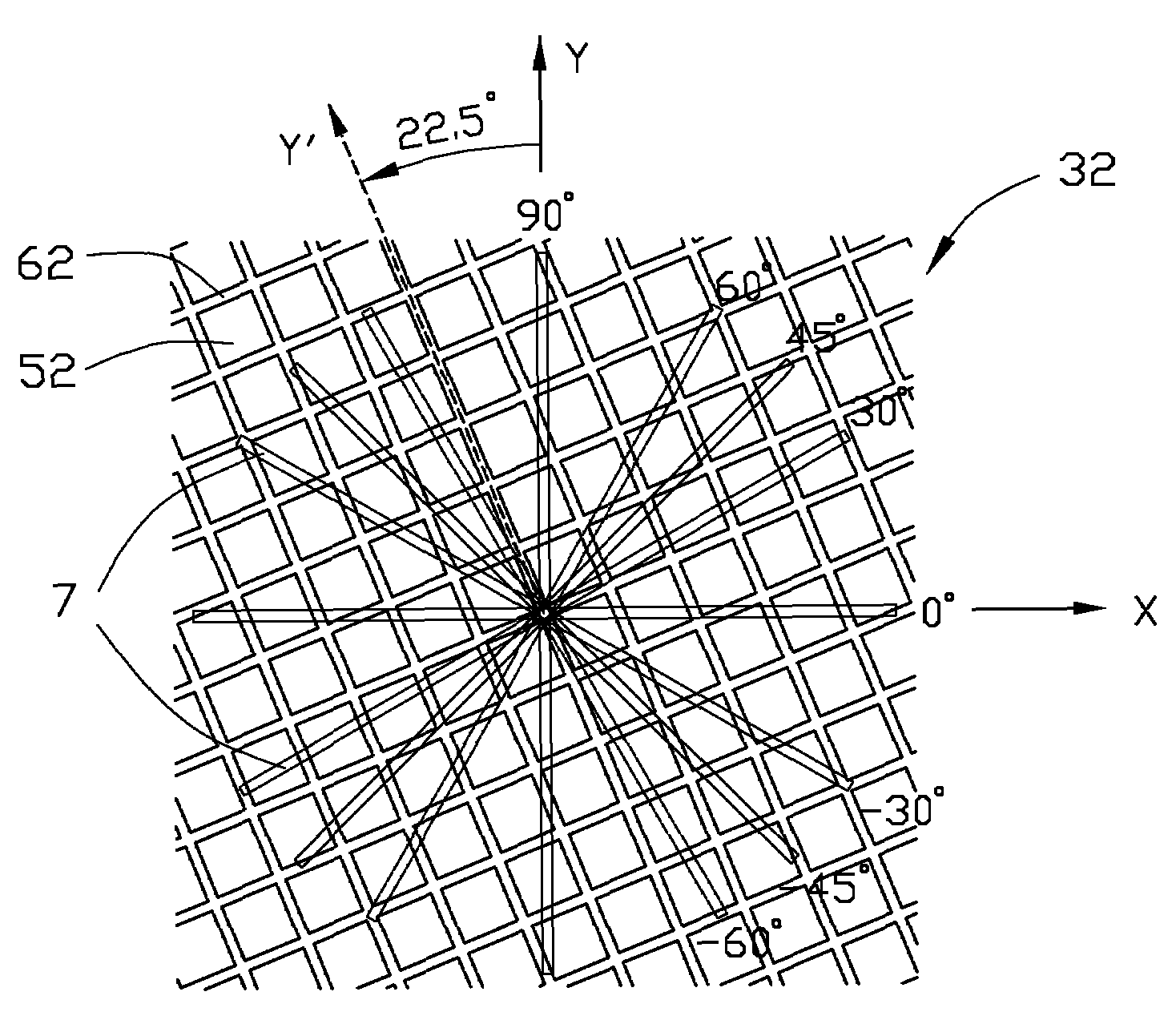
[0020]Referring to FIG. 5, a ground plane 31 in accordance with the present invention is shown. The ground plane 31 includes a plurality of same-sized tiles 51 connected to each other in an array. Each tile 51 is a polygon delimited by six equal straight ground traces 61 connected consecutively end-to-end, forming an equilateral hexagon-shaped tile. The ground plane 31 defines an X-axis along which a straight line segment of a signal trace 7 is arranged. A Y-axis of the ground plane 31 is perpendicular to the X-axis. A straight line passing through one straight ground trace 61 of each tile 51 is designated as a Y′-axis of the tile 51. In the present embodiment, The Y′-axis of each tile 51 is rotated 22.5 degrees relative to the Y-axis of the ground plane 31. Thus, the ground traces 61 are oriented on the ground plane 31 at angles of 22.5, 52.5, 67.5, 112.5, −7.5, −22.5, or −37.5 degrees relative to the X-axis of the ground plane 31. Each straight line segment of the signal traces 7 ...
fourth embodiment
[0024]Referring to FIG. 8, which shows a ground plane 34 of a circuit board in accordance with a In this embodiment, the ground plane 34 includes a plurality of same-sized and generally triangle-shaped tiles 54 with rounded convex corners and rounded concave sides. Each tile 54 is formed by curved ground traces 64.
fifth embodiment
[0025]Referring to FIG. 9, which shows a ground plane 35 of a circuit board in accordance with a In this embodiment, the ground plane 35 includes a plurality of same-sized and generally square-shaped tiles 55 with wavy sides. Each tile 55 is formed by curved ground traces 65.
PUM
 Abstract
Description
Claims
Application Information