System and method for testing semiconductor integrated circuit in parallel

Inactive Publication Date: 2008-07-10
SAMSUNG ELECTRONICS CO LTD
View PDF11 Cites 10 Cited by
  • Summary
  • Abstract
  • Description
  • Claims
  • Application Information

AI Technical Summary

Benefits of technology

[0012]The present invention provides a semiconductor IC testing system having an increased test speed and a high test throughput by testing a plurality of different types of semiconductor DUTs (device under test) in parallel.
[0014]The present invention also provides a semiconductor IC test method for providing an increased test speed and a high test throughput by testing a plurality of different types of semiconductor DUTs in parallel.
[0015]The present invention also provides a semiconductor IC test method that optimally uses resources of an expensive testing system by testing semiconductor DUTs using all the resources of the system.
[0021]Since different types of test programs may be allocated to the circuit sites and run independently, the system according to the present embodiment can test different test items in parallel. Therefore, testing time is shortened, and throughput is increased.

Problems solved by technology

Therefore, the resources of such an expensive system are idled and wasted.

Method used


Image

  • System and method for testing semiconductor integrated circuit in parallel
  • System and method for testing semiconductor integrated circuit in parallel
  • System and method for testing semiconductor integrated circuit in parallel

Examples


Embodiment Construction

[0036]The present invention will now be described more fully with reference to the accompanying drawings, in which exemplary embodiments of the invention are shown.

[0037]In the specification, although terms “a first” and “a second” may be used to describe various members, parts, regions, and / or portions, it is obvious to those skilled in the art that members, parts, regions, and / or portions are not limited by the terms. The terms are used only to identify one member, part, region, or portion. Therefore, a first member, part, region, or portion may designate a second member, part, region, or portion.

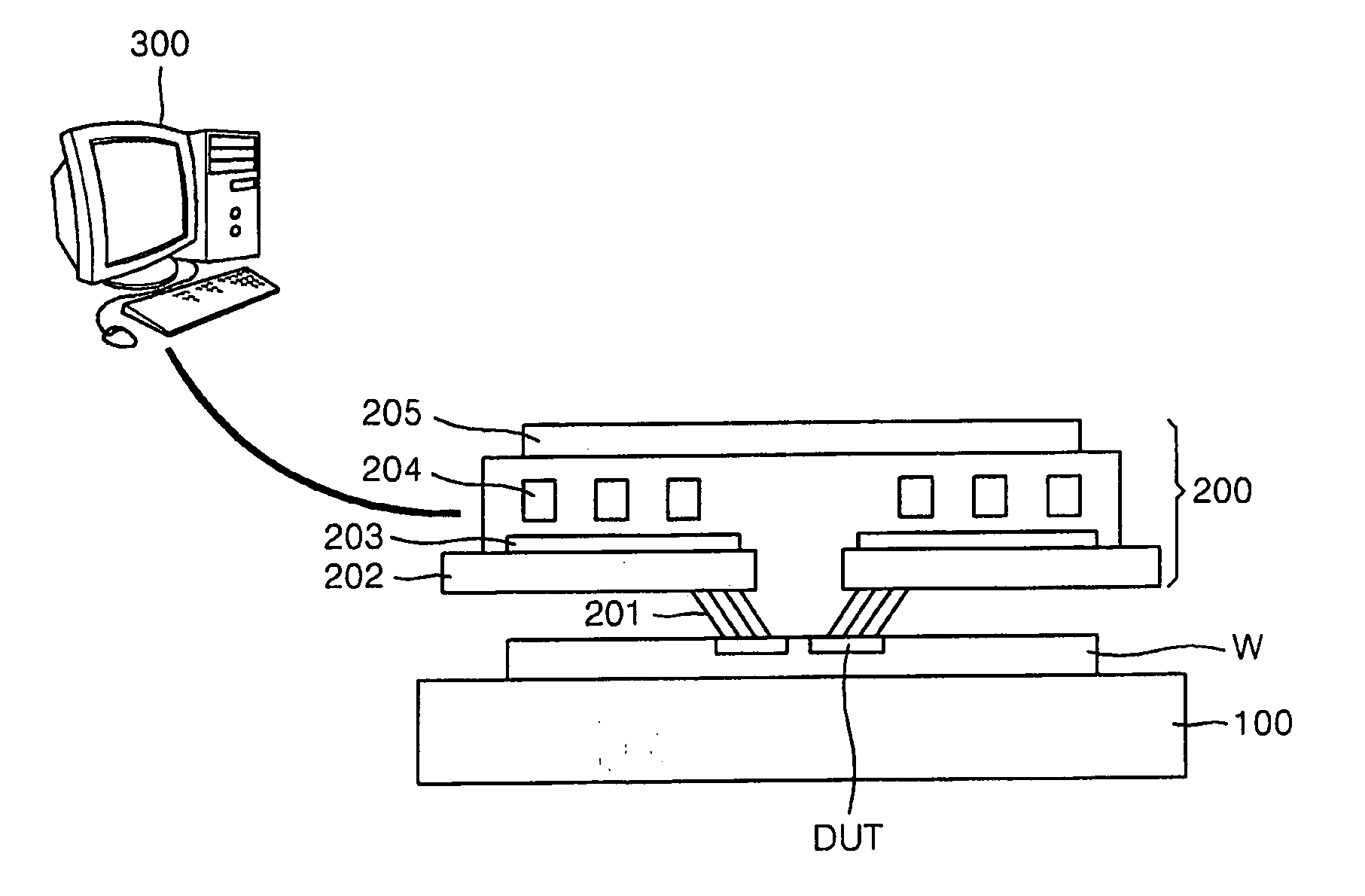
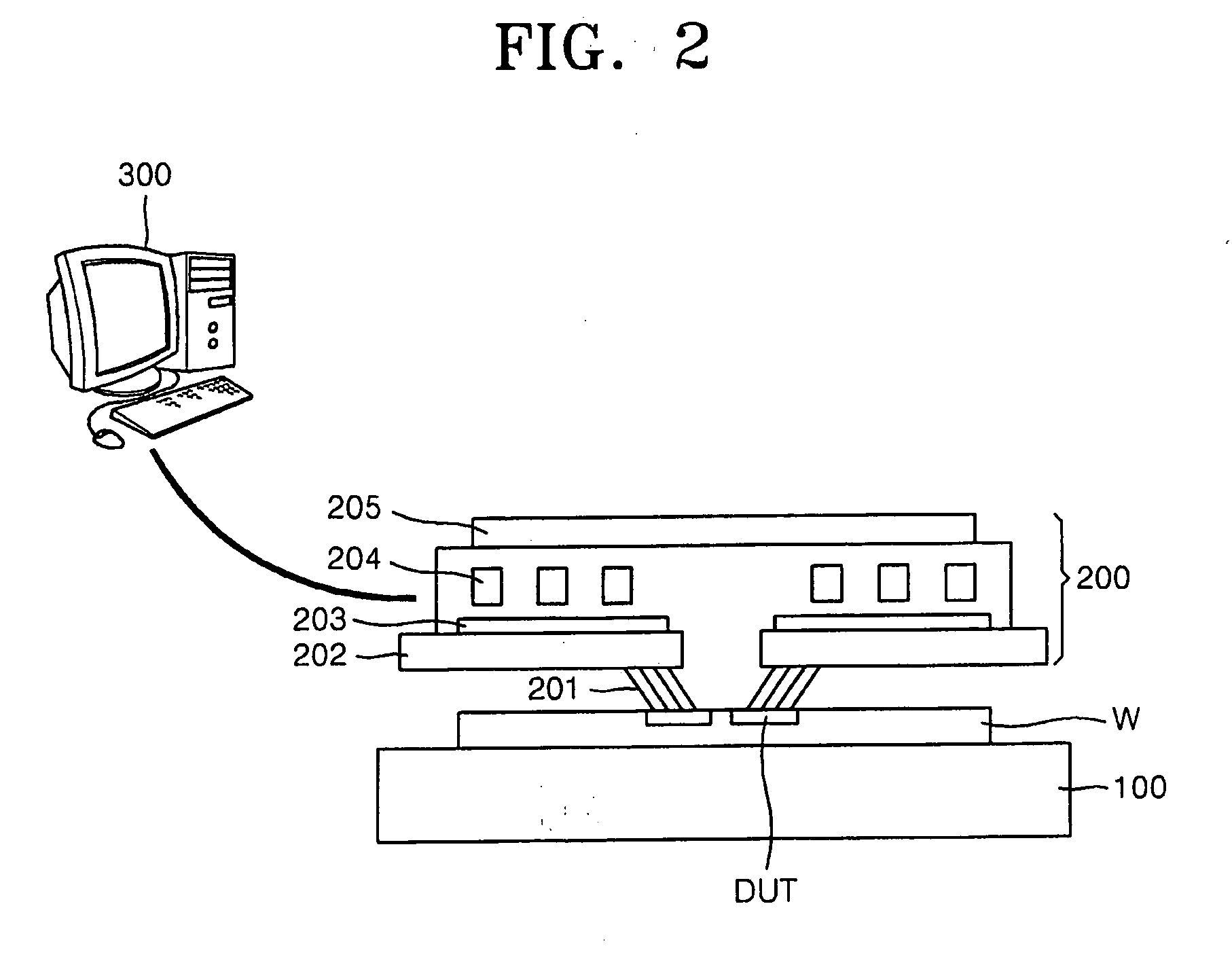
[0038]FIG. 2 is a block diagram illustrating a semiconductor IC testing system for testing semiconductor integrated (IC) chips, according to an embodiment of the present invention.

[0039]Referring to FIG. 2, the parallel type semiconductor IC testing system for parallel testing semiconductor ICs according to the present embodiment includes a probe chuck 100 for loading a wafer W, a test he...


PUM


Abstract

A system and method for testing a semiconductor integrated circuit (IC) in parallel includes a probe chuck, a test head, and a test controller. The probe chuck loads a plurality of different types of semiconductor DUTs. The test head provides a plurality of circuit sites to independently and simultaneously test the different types of semiconductor DUTs, and the test controller controls the test head and the probe chuck.

Description

CROSS-REFERENCE TO RELATED PATENT APPLICATION[0001]This application claims the benefit of Korean Patent Application No. 10-2007-0001183, filed on Jan. 4, 2007, in the Korean Intellectual Property Office, the contents of which are incorporated herein in their entirety by reference.BACKGROUND OF THE INVENTION[0002]1. Field of the Invention[0003]The present invention relates to a system and method for testing a semiconductor integrated circuit (IC) and, more particularly, to a system and method for testing a semiconductor integrated circuit (IC) in parallel.[0004]2. Description of the Related Art[0005]In general, a semiconductor device formed on a semiconductor substrate made of silicon, for example, is manufactured using a sequence of unit processes including a process of stacking layers, a process of doping an impurity, and photolithography and etching processes for patterning the layers. In order to determine whether each of the individual steps is properly performed to manufacture ...

Claims


Application Information

Patent Timeline
IPC IPC(8): G01R31/26
CPCG01R31/2889G01R31/2886H01L22/00
Inventor KIM, MIN-GUAN, YOUNG-SOOCHOI, HO-JEONGKIM, JUNG-HYEON
Owner SAMSUNG ELECTRONICS CO LTD
Why Eureka
Try Eureka