Multilayer type test board assembly for high-precision inspection

Active Publication Date: 2008-07-10
SAMSUNG ELECTRONICS CO LTD
View PDF12 Cites 2 Cited by
  • Summary
  • Abstract
  • Description
  • Claims
  • Application Information

AI Technical Summary

Benefits of technology

[0035]In the multilayer type test board assembly, the mounting devices sensitively influenced by electrical signals are prevented from

Problems solved by technology

In the EDS process, undesirable unit chips of the wafer are sorted and only the unit chips of high quality are subject to subsequent processes.
However, since a conventional test board performs various functions using devices such as an analog-to-digital (A-D) converter, a digital-to-analog (D-A) converter, a micro control unit (MCU), and a measure probe simultaneously, the size of the test board can be excessively large.
Therefore, a sufficient work space is necess

Method used


Image

  • Multilayer type test board assembly for high-precision inspection
  • Multilayer type test board assembly for high-precision inspection
  • Multilayer type test board assembly for high-precision inspection

Examples


Example

[0043]A multiplayer type test board assembly according to the present invention will now be described more fully hereinafter with reference to the accompanying drawings, in which exemplary embodiments of the invention are shown. This invention may, however, be embodied in different forms and should to not be construed as limited to the embodiments set forth herein.

[0044]It will also be understood that when an element such as a layer, region or substrate is referred to as being on another element, it can be directly on the other element or intervening elements may also be present, or it can be partially or completely in the other element. In contrast, if an element is referred to as being directly on another element, then no other intervening elements are present.

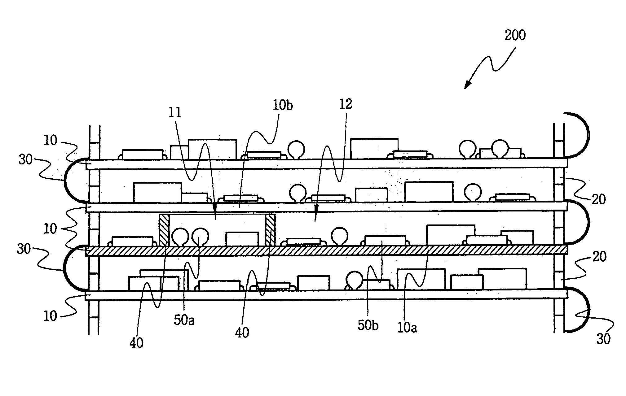
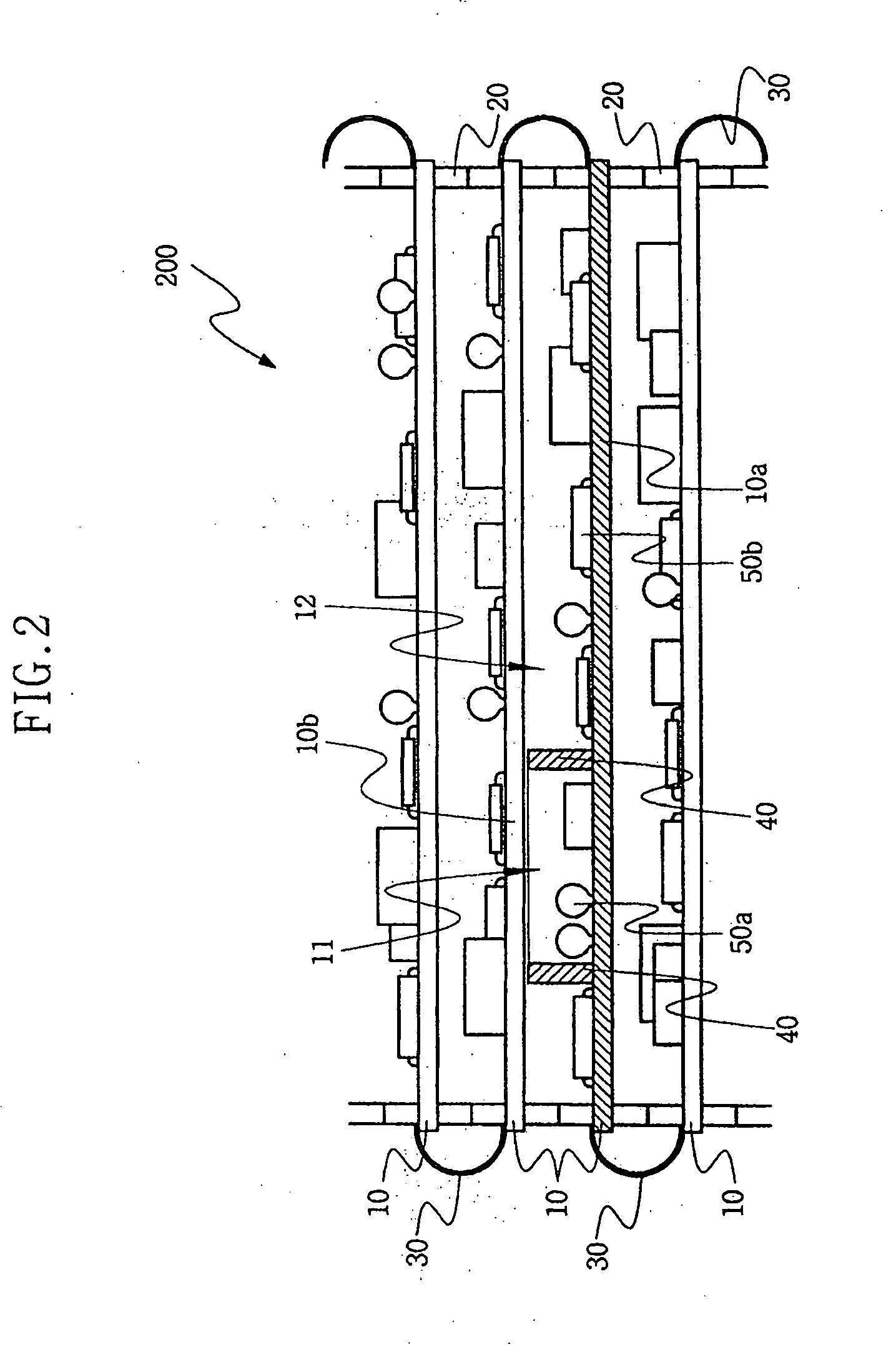
[0045]FIG. 2 is a schematic side sectional view of a multilayer type test board assembly 200 for high-precision inspection according to an embodiment of the present invention.

[0046]As shown in FIG. 2, a multilayer type test ...


PUM


Abstract

There is provided a multilayer type test board assembly for high-precision inspection. The multilayer test board assembly comprises: a plurality of test boards separated from each other according to their functions, having input/output signal terminals, and including at least one test board each having a first section where first mounting devices sensitive to an influence of electrical signals are mounted and a second section where second mounting devices insensitive to an influence of electrical signals are mounted; spacers that arrange the test boards in parallel by spacing apart the test boards by predetermined intervals; connection cables connected to the input/output signal terminals of the test boards; and a signal shielding fence formed on each of the at least one test board so as to protect the first mounting devices from electrical signals generated by the second mounting devices.

Description

CROSS-REFERENCE TO RELATED APPLICATION[0001]This application claims the benefit of Korean Patent Application No. 10-2007-0000933, filed in the Korean Intellectual Property Office on Jan. 4, 2007, the contents of which are hereby incorporated herein by reference in their entirety.BACKGROUND OF THE INVENTION[0002]1. Field of the Invention[0003]The present invention relates to a multilayer type test board assembly for high-precision inspection, and more particularly to a test board assembly for high-precision inspection capable of measuring a micro current and a low current by safely protecting the test board assembly from an influence of external signals.[0004]2. Description of the Related Art[0005]In general, a semiconductor device is manufactured by a fabrication process that includes forming patterns on a wafer and an assembling process that includes assembling the wafer having the patterns into unit chips.[0006]An electric die sorting (EDS) process is performed between the fabrica...

Claims


Application Information

Patent Timeline
IPC IPC(8): G01R1/02
CPCG01R1/04G01R31/2851H05K1/144H05K2201/10371H05K2201/042H05K2201/09972H05K1/148H01L22/00
Inventor KIM, MIN-GUAN, YOUNG-SOOCHOI, HO-JEONGKIM, JUNG-HYEON
Owner SAMSUNG ELECTRONICS CO LTD
Why Eureka
Try Eureka