Semiconductor device and method of fabricating the same

Active Publication Date: 2008-07-17
VALLEY DEVICE MANAGEMENT
View PDF6 Cites 46 Cited by
  • Summary
  • Abstract
  • Description
  • Claims
  • Application Information

AI Technical Summary

Benefits of technology

[0010]The present invention has been made taking the above into consideration and has an object of providing a semiconductor devic

Problems solved by technology

In addition, the conventional semiconductor device has large financial and time burdens because it needs a metal mold for the resin seal portion 24 that matches in size with t

Method used


Image

  • Semiconductor device and method of fabricating the same
  • Semiconductor device and method of fabricating the same
  • Semiconductor device and method of fabricating the same

Examples


Example

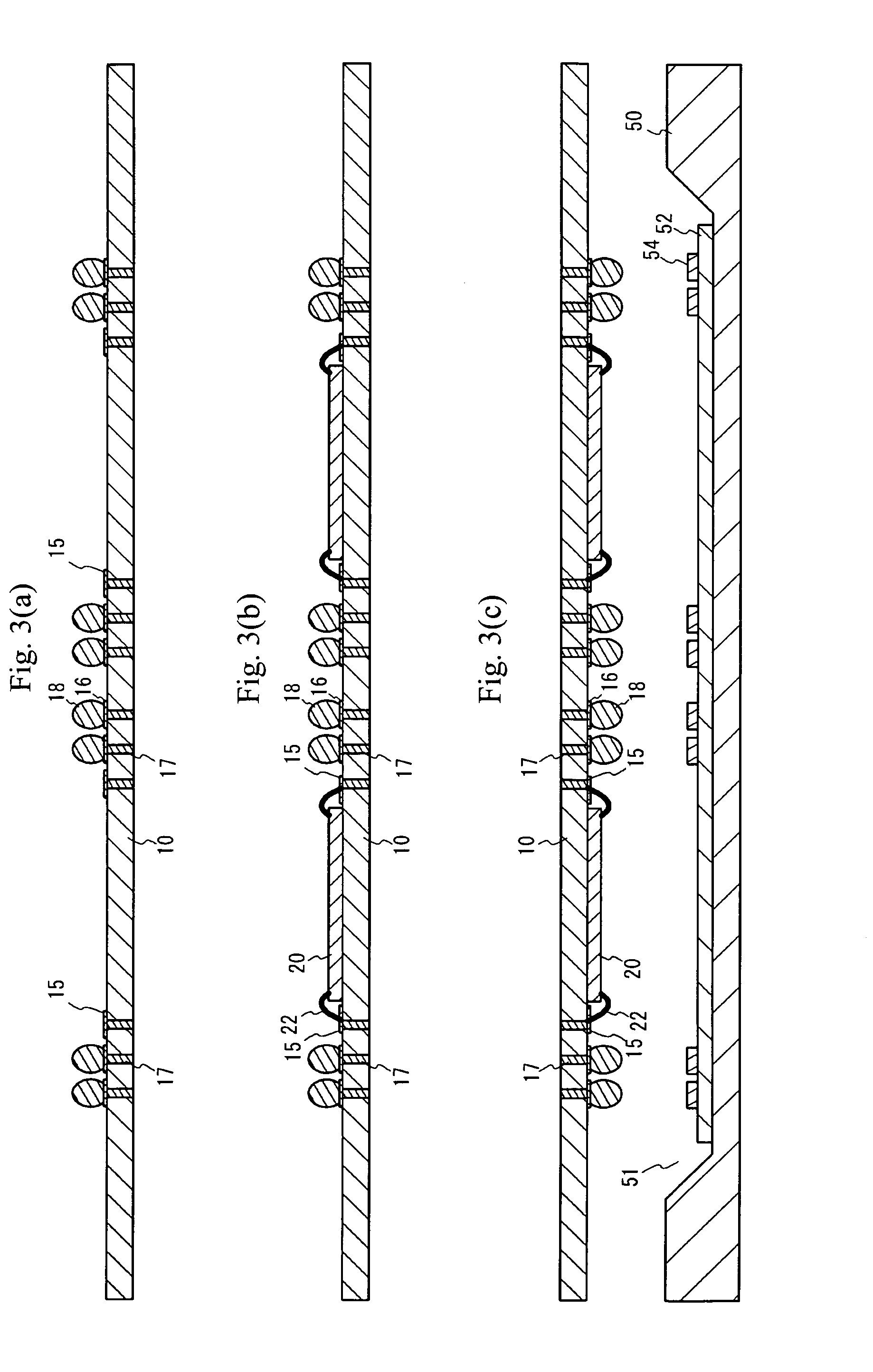
[0040]A first embodiment is an exemplary built-in semiconductor device for stacking. A description is now given of a method of fabricating the semiconductor device of the first embodiment with reference to FIGS. 3(a) through 4(c). Multiple semiconductor chips are mounted on the wiring substrate 10 in a transverse direction. In FIGS. 3(a) through 4(c), only two semiconductor chips 20 are illustrated for the sake of simplicity. Referring to FIG. 3(a), the land electrodes 16 are formed on the wiring substrate 10 that may be a printed-circuit board made of glass epoxy resin. The semiconductor balls 18, which may be slightly higher than 300 μm, are formed on the land electrodes 16. Referring to FIG. 3(b), the semiconductor chips 20, which may be 100 μm thick, are mounted on the wiring substrate 10 by using an adhesive. The wires 22 are provided to make electrical connections between semiconductor chips 20 and the pads 15 on the wiring substrate 10. Referring to FIG. 3(c), a metal mold 50...

Example

Second Embodiment

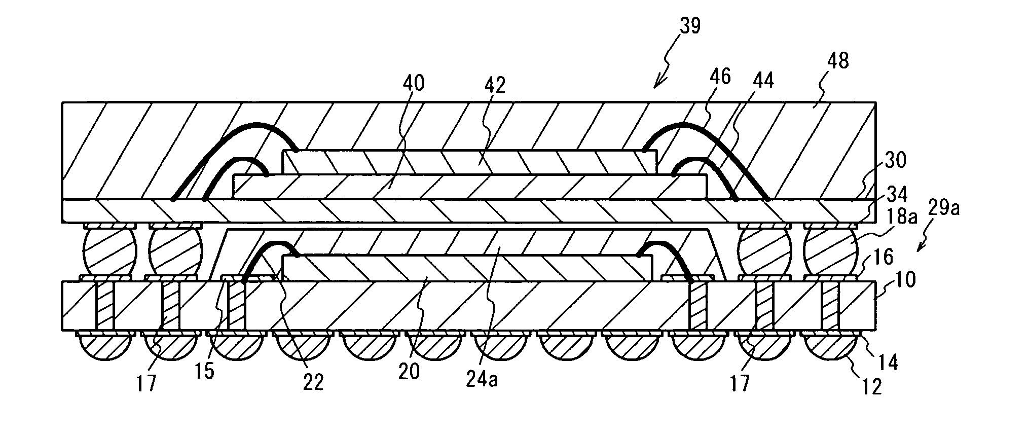
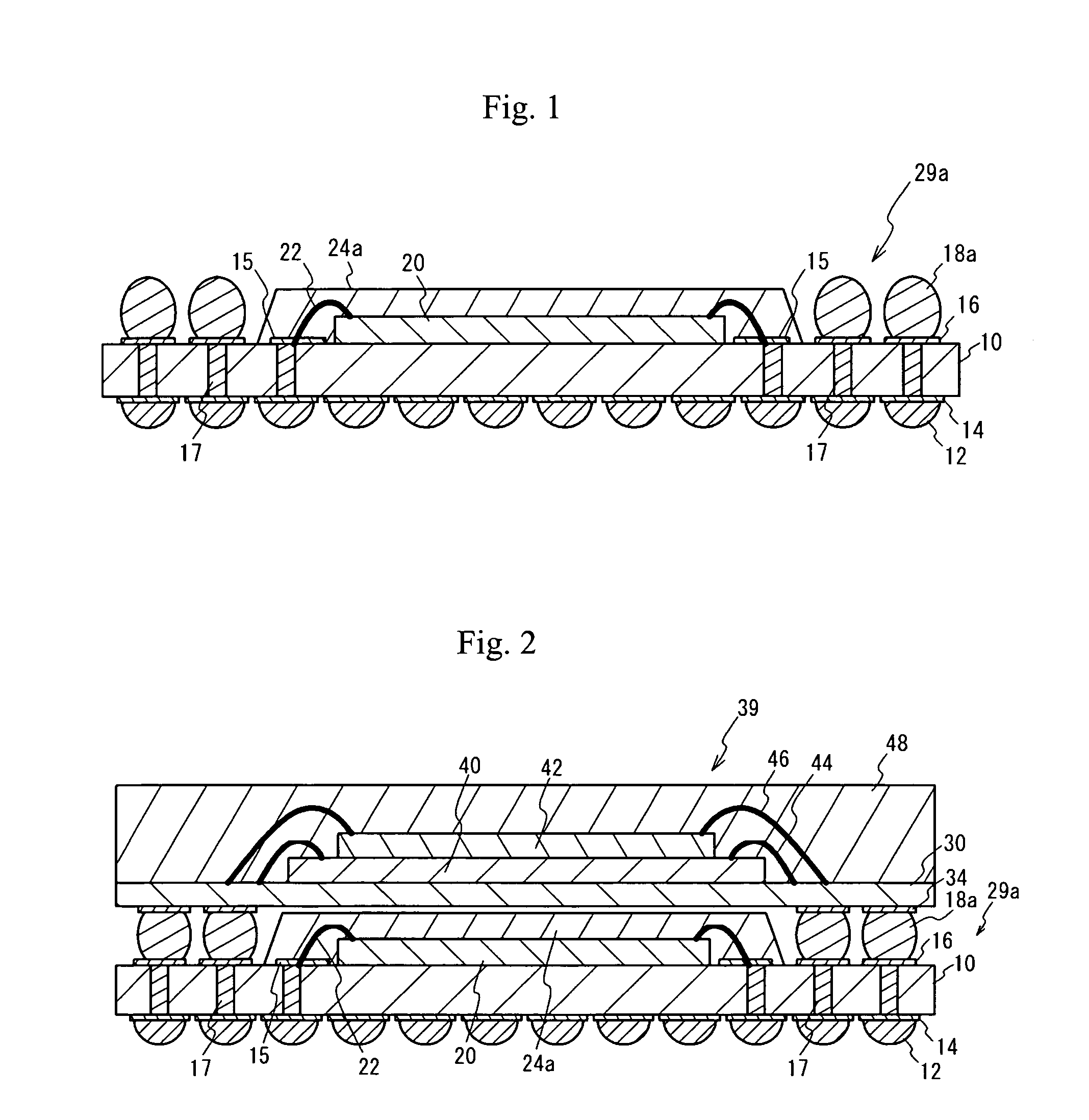
[0043]A second embodiment has an exemplary arrangement in which a semiconductor device is stacked on the built-in semiconductor device in accordance with the first embodiment. FIG. 6 is a cross-sectional view of a method of fabricating a semiconductor device in accordance with the second embodiment. One built-in semiconductor device of the first embodiment is arranged as a lower semiconductor device 29, and the upper semiconductor device 39 employed in the aforementioned related art is arranged on the lower semiconductor device 29. In this arrangement, solder balls 32 of the upper semiconductor device 39 are fit into the openings 25 formed in the resin seal portion 24 of the lower semiconductor device 29. Then, the lower semiconductor device 29 and the upper semiconductor device 39 are heated to melt the solder balls 18 and 32, so that the semiconductor device of the second embodiment can be completed.

[0044]FIG. 7 is a cross-sectional view of a semiconductor device ...

Example

Third Embodiment

[0053]A third embodiment is an exemplary device in which the solder balls 18 of the lower semiconductor device 29 are formed in a manner different from the above-mentioned manner. A description is now given, with reference to FIG. 8(a) through 9(b), of a method of fabricating a semiconductor device in accordance with the third embodiment. Referring to FIG. 8(a), the processes shown in FIGS. 3(a) and 3(b) in association with the first embodiment are carried out. Referring to FIG. 8(b), the metal mold 50 is disposed which has the molding portion 51 for shaping the resin seal portion 24 on the side of the wiring substrate 10 on which the semiconductor chip 20 is arranged. A sheet 53 that is softer than the solder balls 18 is arranged. Thermoset epoxy region 56 is given to the molding portion 51 of the metal mold 50 in an uncured state. The metal mold 50 is heated to approximately 175° C. to melt the epoxy resin. Referring to FIG. 8(c), the wiring substrate 10 and the me...


PUM


Abstract

A method of fabricating a semiconductor device includes: mounting a semiconductor chip on a substrate; forming an upper connection terminal on a side of the substrate on which the semiconductor chip is mounted; forming a resin seal portion that seals the semiconductor chip and the upper connection terminal so that an upper surface of the upper connection terminal is exposed; and shaping the upper connection terminal so that the upper surface of the upper connection terminal becomes lower than an upper surface of the resin seal portion.

Description

CROSS-REFERENCES TO RELATED APPLICATIONS[0001]This is a continuation-in-part of International Application No. PCT / JP2006 / 300542, filed Jan. 17, 2006 which was not published in English under PCT Article 21(2).BACKGROUND OF THE INVENTION[0002]1. Field of the Invention[0003]The present invention generally relates to a semiconductor device and a method of fabricating the semiconductor device, and more particularly, to a semiconductor device having multiple built-in semiconductor devices stacked and a method of fabricating the semiconductor device.[0004]2. Description of the Related Art[0005]In recent years, there is a demand to downsize semiconductor devices used as non-volatile storage media for portable electronic devices such as portable phones and IC memory cards. It is particularly demanded to package semiconductor chips efficiently. One of the packaging techniques is to stack packages (built-in semiconductor devices) each having a semiconductor chip.[0006]Referring to FIGS. 1 and ...

Claims


Application Information

Patent Timeline
IPC IPC(8): H01L23/02H01L21/00
CPCH01L21/561H01L2225/1058H01L23/3128H01L24/97H01L25/105H01L2224/16225H01L2224/32145H01L2224/48091H01L2224/48227H01L2224/97H01L2924/01004H01L2924/01029H01L2924/0103H01L2924/01079H01L2924/01082H01L2924/14H01L2924/15311H01L2924/1532H01L2924/15331H01L21/568H01L2924/3511H01L2224/73265H01L2224/73204H01L2224/32225H01L2225/1023H01L24/48H01L2924/01005H01L2924/01006H01L2924/01033H01L2224/85H01L2924/00014H01L2924/00012H01L2924/00H01L24/73H01L2924/181H01L2224/45099H01L2224/45015H01L2924/207
Inventor TANAKA, JUNJIKASAI, JUNICHIMEGURO, KOUICHIONODERA, MASANORITAYA, KOJI
Owner VALLEY DEVICE MANAGEMENT
Why Eureka
Try Eureka