Method of manufacturing a semiconductor device

Inactive Publication Date: 2005-02-03
HITACHI LTD +1
View PDF4 Cites 7 Cited by
  • Summary
  • Abstract
  • Description
  • Claims
  • Application Information

AI Technical Summary

Benefits of technology

[0008] It is an object of the present invention to provide for the manufacturing of semiconductor devices of the resin mold type, in which multiple semiconductor chips which are mounted on a wiring substrate are processed for block molding and

Problems solved by technology

However, this manner necessitates an awkward work of forming on the molding die different patterns of address informati

Method used


Image

  • Method of manufacturing a semiconductor device
  • Method of manufacturing a semiconductor device
  • Method of manufacturing a semiconductor device

Examples


embodiment 1

[0038] Embodiment 1

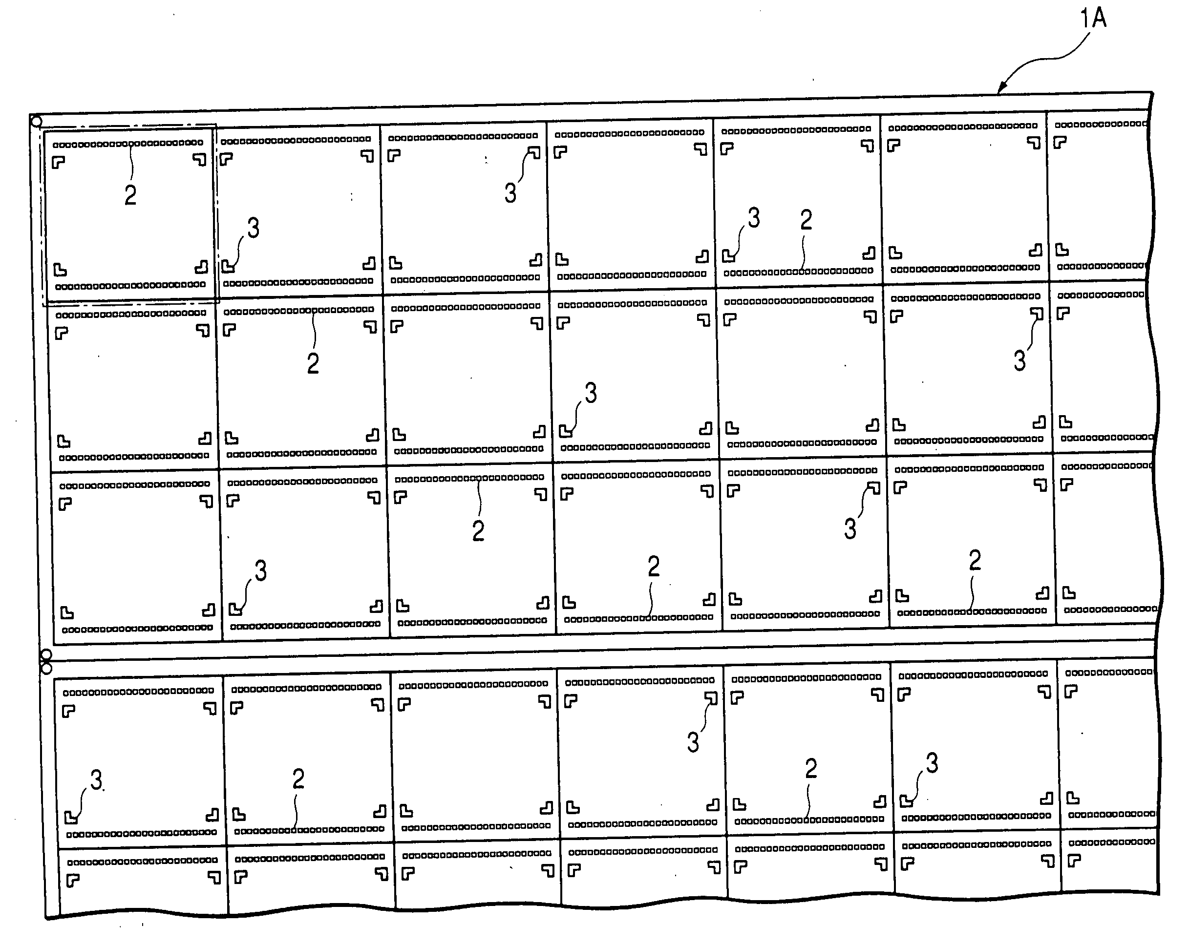
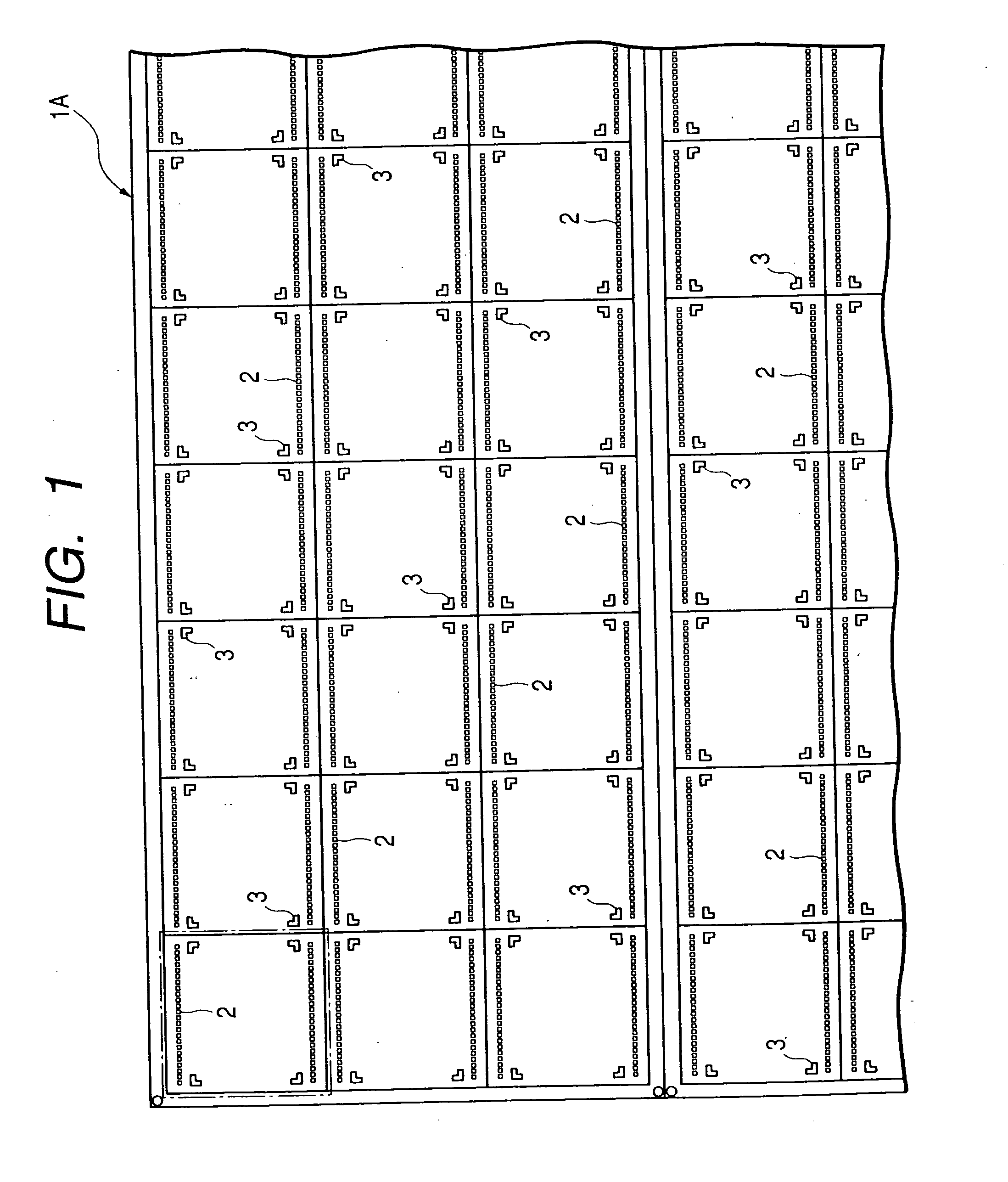
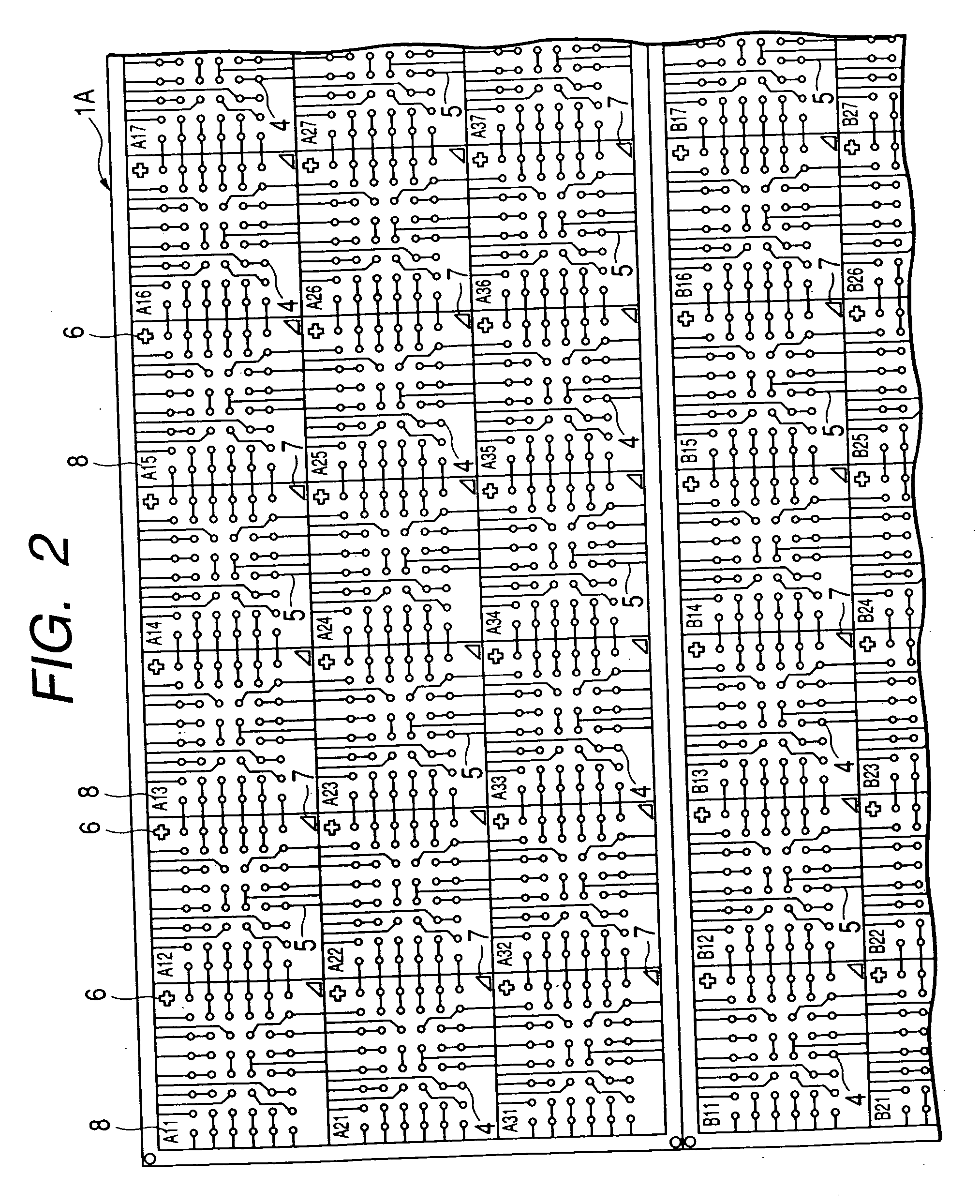
[0039]FIG. 1 and FIG. 2 show part of the matrix substrate which is used for the manufacturing of resin-molded semiconductor devices based on this embodiment. FIG. 1 shows the chip mounting surface (upper side), and FIG. 2 shows the packaging surface (rear side).

[0040] The matrix substrate 1A is a thin wiring substrate of resin having dimensions of 500 mm by 500 mm and 0.22 to 0.6 mm in thickness, for example, on the upper side of which are mounted a plurality of semiconductor chips in a matrix arrangement in the pellet putting process which will be explained later. The matrix-substrate 1A is made of a known material for wiring substrates, e.g., glass epoxy resin, BT resin or polyamide resin, and particularly it can be made of such an inexpensive material for wiring substrates as glass epoxy resin thereby to lower the manufacturing cost of resin-molded semiconductor devices. The matrix substrate 1A can also be made of a wiring substrate having flexibility such as ...

embodiment 2

[0061] Embodiment 2

[0062] The address information patterns 8, which are formed by use of the wiring material on the packaging surface of the matrix substrate 1A in the preceding embodiment 1, can be formed in a different manner as follows.

[0063] Initially, a matrix substrate 1A as shown in FIG. 19 is prepared. This matrix substrate 1A has the same structure as the matrix substrate 1A of the preceding embodiment 1 except that it does not have the address information patterns 8.

[0064] Next, the processing steps of the preceding embodiment 1 shown in FIG. 6 through FIG. 11 are followed to implement the cutting out of matrix substrates 1B for molding, bonding of wires 13, and block molding of chips 12 with the resin mold 14. Finally, marks 19 of the product type, lot number, etc. are printed on the surface of the resin mold 14, and, at the same time in this embodiment, address information patterns 8 are printed on the surface of the resin mold 14 as shown in FIG. 20. The marks 19 and ...


PUM


Abstract

For the manufacturing of semiconductor devices, in which multiple semiconductor chips which are mounted on a wiring substrate are processed for block molding and thereafter the wiring substrate is diced into individual resin-molded semiconductor devices, here is disclosed a technique for finding out easily, even after the dicing process, the position of each resin-molded semiconductor device in its former state on the wiring substrate. It includes processing steps of implementing the block molding with resin for multiple semiconductor chips mounted on a wiring substrate and thereafter dicing the wiring substrate into individual resin-molded semiconductor devices, with the substrate dicing step being preceded by a step of appending an address information pattern to each of the resin-molded semiconductor devices.

Description

BACKGROUND OF THE INVENTION [0001] The present invention relates to the technology of the manufacturing of semiconductor devices, and particularly to a technique which is useful for the manufacturing of semiconductor devices of the resin mold type in which multiple semiconductor chips mounted on a wiring substrate are processed for block molding and thereafter the wiring substrate is diced into individual semiconductor devices. [0002] Japanese Patent Unexamined Publication No. Hei 11(1999)-214588 describes a method of manufacturing semiconductor devices of the resin mold type in which multiple semiconductor chips mounted on a TAB tape are molded with resin and thereafter the resin and TAB tape are cut into individual semiconductor devices. [0003] The above-mentioned patent publication also discloses a technique for preventing the displacement of the cutting position of the resin and TAB tape based on the accurate observation of the cutting position which is displayed in terms of the...

Claims


Application Information

Patent Timeline
IPC IPC(8): H01L21/56H01L23/28H01L23/00H01L23/31
CPCH01L21/561H01L2924/10253H01L23/3128H01L24/97H01L2223/54406H01L2223/54473H01L2223/54486H01L2224/32225H01L2224/48091H01L2224/48227H01L2224/73265H01L2224/97H01L2924/01004H01L2924/01029H01L2924/01047H01L2924/01078H01L2924/01079H01L2924/01082H01L2924/01322H01L2924/15311H01L24/48H01L2924/01005H01L2924/01006H01L2924/01033H01L2224/45144H01L2224/45147H01L21/565H01L2924/00014H01L2224/85H01L2224/83H01L2224/92247H01L2924/00012H01L2924/00H01L2924/12042H01L24/45H01L24/73H01L2924/181H01L2224/85203H01L2224/85205H01L2924/00015H01L2224/05599H01L23/00H01L21/44
Inventor WADA, TSUTOMUMASUDA, MASACHIKA
Owner HITACHI LTD
Why Eureka
Try Eureka