Stack type semiconductor chip package having different type of chips and fabrication method thereof

a stack type and chip technology, applied in the direction of semiconductor devices, semiconductor devices, electrical equipment, etc., can solve the problems of undesirable complex rewiring layout of limited performance improvement of conventional stack type semiconductor chip packages of fig. 1, and inability to use image sensor chip packages as stack type semiconductor chip packages, etc., to achieve easy fabrication of stack types and minimize package dimensions , improve package performance and fabrication yield

Active Publication Date: 2008-07-17
SAMSUNG ELECTRONICS CO LTD
View PDF3 Cites 82 Cited by
  • Summary
  • Abstract
  • Description
  • Claims
  • Application Information

AI Technical Summary

Benefits of technology

[0013]The present invention provides a stack type semiconductor chip package that is applicable to an image sensor chip package, and can improve package performance and fabrication yield.
[0014]The present invention also provides a fabrication method for easily fabricating a stack type semiconductor chip package as described above.
[0015]According to an aspect of the present invention, there is provided a stack type semiconductor chip package including a first wafer mold, a protection substrate, and a second wafer mold that are stacked in a wafer level process. The first wafer mold includes a first chip having first pads on one surface, and a first mold layer surrounding and encapsulating the first chip. The protection substrate is placed on the first wafer mold, is mechanically bonded with the first wafer mold using a first adhesive layer interposed therebetween, and includes wiring layers on one surface facing the first pads to be electrically connected to the first wafer mold. The second wafer mold includes a second chip having second pads on one surface, and a second mold layer surrounding and encapsulating the second chip. First and second vias electrically connect the first and second chips, the protection substrate, and external connection terminals. Accordingly, the first and second chips are directly connected without bonding wires, thereby minimizing the package dimensions and increasing the fabrication yield compared to the conventional art. Also, a stack type semiconductor chip package according to the present invention is suitable for use as an image sensor chip package.

Problems solved by technology

However, performance improvement of the conventional stack type semiconductor chip package of FIG. 1 is limited since the different types of chips 12, 14 and 16 are indirectly connected to one another through the PCB 10 using the bonding wires 18.
Furthermore, the stack type semiconductor chip package of FIG. 1 cannot be used as an image sensor chip package because image sensor chip packages are sensitive to impurity particles due to factors related to the packaging process.
However, the stack type semiconductor chip package of FIG. 2 has an undesirably complex rewiring layout.
Additionally, the stack type semiconductor chip package of FIG. 2 must disadvantageously employ the interposer chip 32.
The stack type semiconductor chip package of FIG. 2 has many structural problems such as structural instability resulting from stacking larger chips 36 and 38 on a smaller chip 34.
The stack type semiconductor chip package of FIG. 2 also cannot be used for an image sensor chip package that is sensitive to impurity particles such as dust because of factors related to the packaging process.

Method used


Image

  • Stack type semiconductor chip package having different type of chips and fabrication method thereof
  • Stack type semiconductor chip package having different type of chips and fabrication method thereof
  • Stack type semiconductor chip package having different type of chips and fabrication method thereof

Examples


Embodiment Construction

[0022]The present invention will now be described more fully with reference to the accompanying drawings, in which exemplary embodiments of the invention are shown. The invention may, however, be embodied in many different forms and should not be construed as being limited to the embodiments set forth herein; rather, these embodiments are provided so that this disclosure will be thorough and complete, and will fully convey the concept of the invention to those skilled in the art. In the drawings, the thicknesses and sizes of layers and regions are exaggerated for clarity.

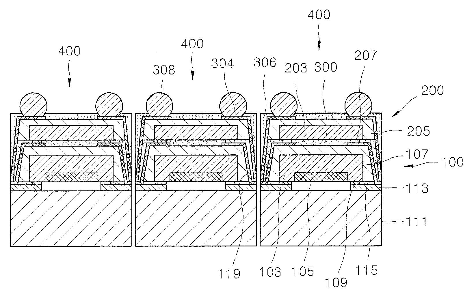
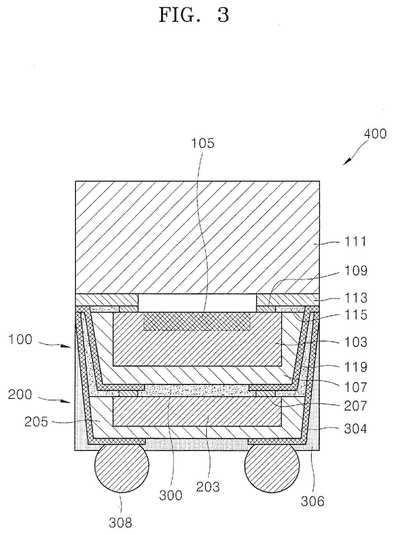
[0023]A stack type semiconductor chip package according to embodiments of the present invention includes different types of chips stacked in a wafer level. The different types of chips have different functions and sizes, and may be a memory circuit chip, a logic circuit chip, an image sensor chip, and an image signal processor (ISP). Although two different types of chips are stacked in a present embodiment, stacking...


PUM


Abstract

A stack type semiconductor chip package includes a first wafer mold, a protection substrate, and a second wafer mold that are stacked in a wafer level process. The first wafer mold includes a first chip having first pads and a first mold layer encapsulating the first chip. The protection substrate is placed on the first wafer mold, is mechanically bonded with the first wafer mold using a first adhesive layer, and includes wiring layers facing the first pads. The second wafer mold is placed under the first wafer mold, is mechanically bonded with the first wafer mold using a second adhesive layer, and includes a second chip having second pads, and a second mold layer encapsulating the second chip. First vias electrically connect the wiring layers of the protection substrate with the second pads. Second vias electrically connect the wiring layers of the protection substrate with external connection terminals.

Description

CROSS-REFERENCE TO RELATED PATENT APPLICATION[0001]This application claims priority under 35 USC § 119 to Korean Patent Application No. 10-2007-0004412, filed on Jan. 15, 2007 in the Korean Intellectual Property Office, the disclosure of which is incorporated herein in its entirety by reference.BACKGROUND[0002]1. Technical Field[0003]The present invention relates to a stack type semiconductor chip package and a fabrication method thereof, and more particularly, to a stack type semiconductor chip package having different types of chips, and a fabrication method thereof.[0004]2. Description of the Related Art[0005]As a variety of semiconductor products are developed, a stack type semiconductor chip package (for instance, a multichip package (MCP)) or a system in package (SIP), including different types of chips stacked on top of one another, are being used for a semiconductor package.[0006]FIG. 1 is a cross-sectional view illustrating one example of a conventional stack type semicondu...

Claims


Application Information

Patent Timeline
Patent Type & Authority Applications(United States)
IPC IPC(8): H01L23/488H01L21/56
CPCH01L21/561H01L2924/01006H01L24/48H01L24/96H01L24/97H01L25/0657H01L27/14618H01L31/0203H01L2224/32145H01L2224/32225H01L2224/48091H01L2224/48227H01L2224/484H01L2224/73265H01L2224/97H01L2225/06524H01L2225/06551H01L2924/01014H01L2924/01022H01L2924/01028H01L2924/01029H01L2924/01047H01L2924/0105H01L2924/01078H01L2924/01079H01L2924/01082H01L2924/014H01L2924/15311H01L21/568H01L2924/01033H01L2224/12105H01L2924/00014H01L2924/00H01L2924/15788H01L2924/181H01L2224/13025H01L2224/04105H01L2224/45099H01L2224/05599H01L2924/00012H01L23/12H01L23/48
Inventor KWON, WOON-SEONGKWON, YONG-HWANKANG, UN-BYOUNGLEE, CHUNG-SUNJANG, HYUNG-SUN
Owner SAMSUNG ELECTRONICS CO LTD
Why Eureka
Try Eureka