Optoelectronic device in combination with a push-in cage

a technology of optoelectronic devices and push-in cages, which is applied in the direction of coupling device connections, electrical apparatus construction details, instruments, etc., can solve the problems of circuit board rework, and achieve the effect of occupying as much area and being easy to mated

Inactive Publication Date: 2008-07-17
STRATOS INT
View PDF27 Cites 12 Cited by
  • Summary
  • Abstract
  • Description
  • Claims
  • Application Information

AI Technical Summary

Benefits of technology

[0018]Thus, the invention achieves the objectives set forth above. The invention provides a device which is able to be easily mated to a host structure, does not take up as much area on a circuit board of a host structure as compared to other optoelectronic devices, does not require a cage mounted to the circuit board of the host structure, and which does not require as much work to be performed on the circuit board of the host structure so as to enable the host structure to interact with the device.

Problems solved by technology

Also, when the cage is mounted to the circuit board of the host structure, errors, mistakes, or accidents can cause the act of attaching the cage to the circuit board to ruin or cause the circuit board to be reworked.

Method used


Image

  • Optoelectronic device in combination with a push-in cage
  • Optoelectronic device in combination with a push-in cage
  • Optoelectronic device in combination with a push-in cage

Examples


Embodiment Construction

[0040]Referring now to the drawings, wherein like reference numerals designate identical or corresponding parts throughout the several views, and more particularly to FIGS. 1-20 thereof, an embodiment of the present invention is displayed therein.

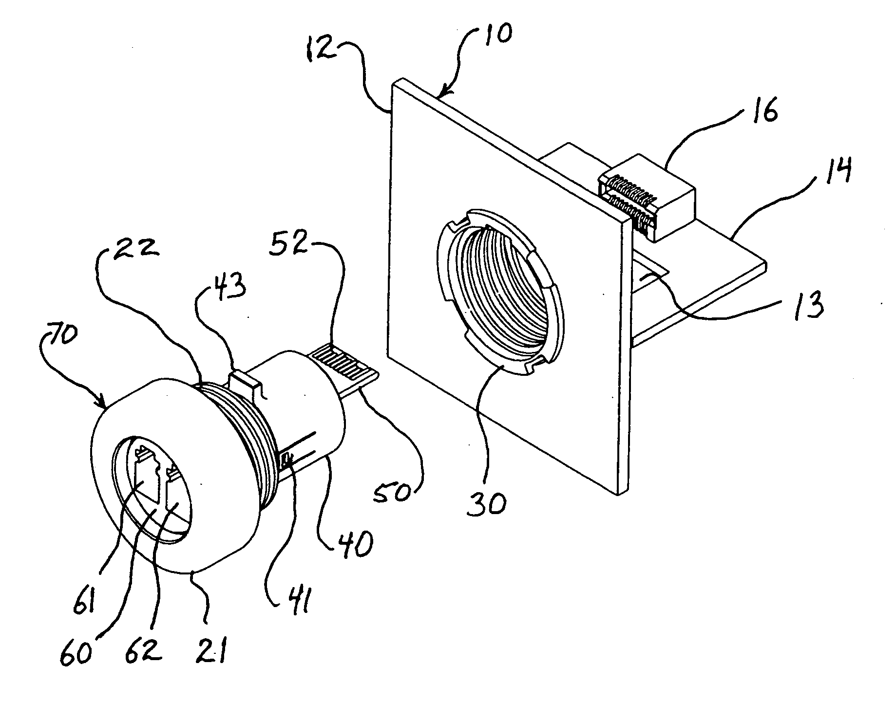
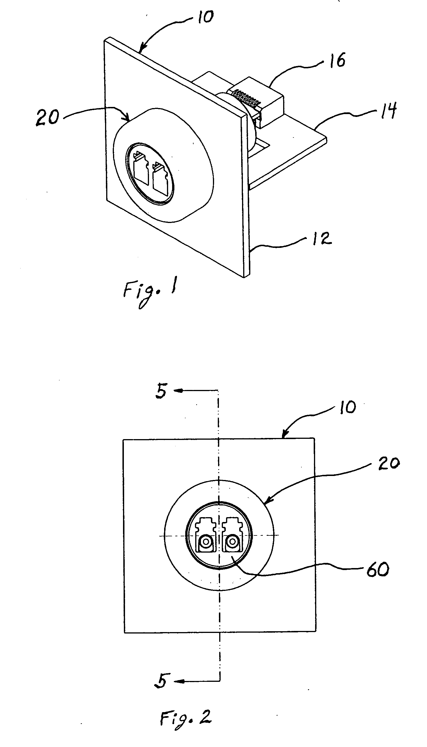
[0041]FIG. 1 is a perspective view of an embodiment of a device 20 mated to a portion of a host structure 10. The portion of the host structure 10 includes a bezel or faceplate 12, a circuit board 14, and an electrical connector 16 attached to the circuit board 14. The device 20 includes an optoelectronic device 70 and a push-in cage 30 (see FIG. 3).

[0042]FIG. 2 is a front view of the device 20 mated to the host structure 10 of FIG. 1. An optical connector 60 of the device 20 is disclosed. As shown, the optical connector 60 includes two optical ports.

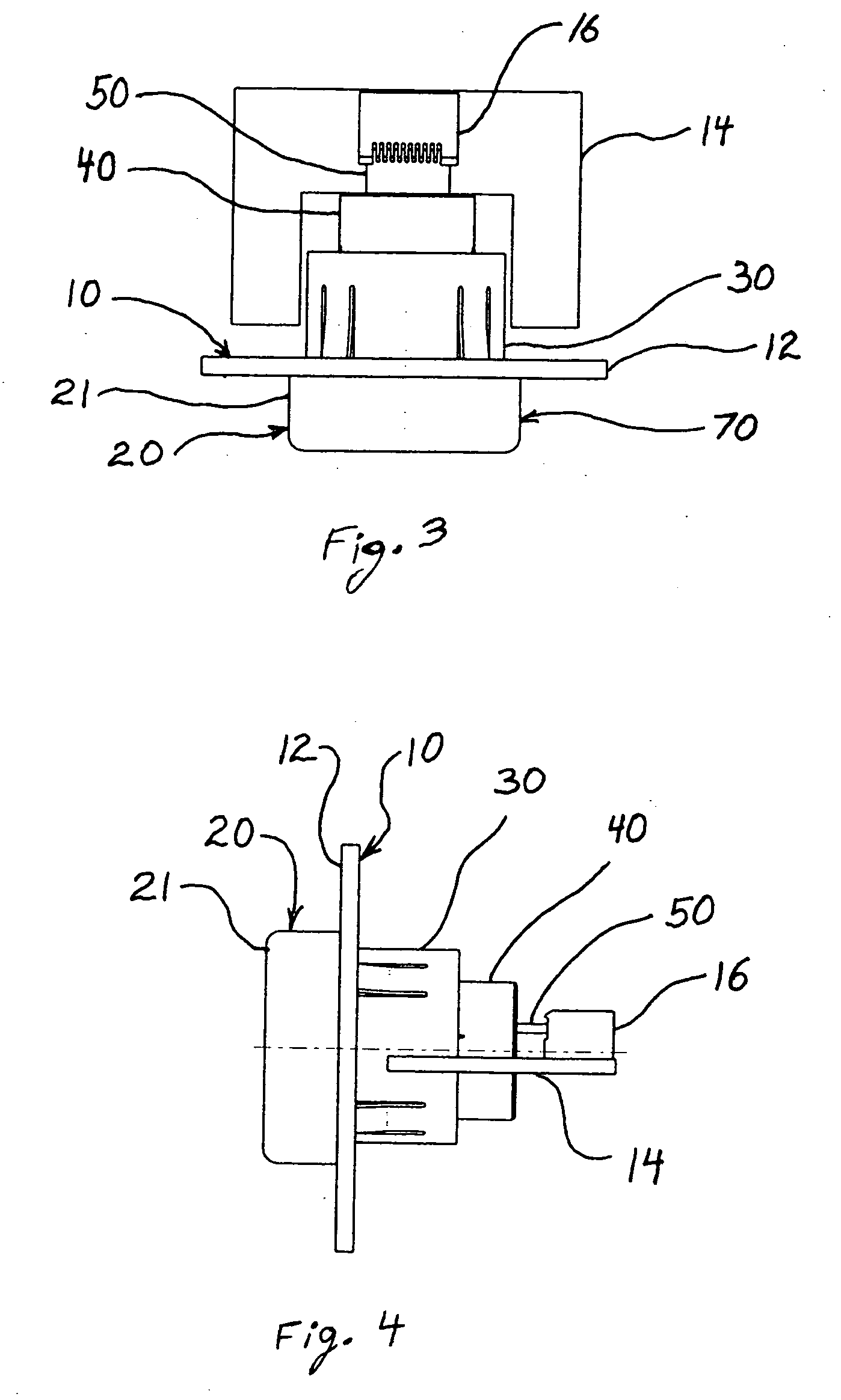
[0043]FIG. 3 is a top view of the device 20 mated to the host structure 10. FIG. 4 is a side view of the device 20 mated to or engaged with the host structure 10. The faceplate 12, the circuit ...


PUM


Abstract

The device includes a push-in cage, and an optoelectronic device. The push-in cage includes a first thread form, and a first key. The optoelectronic device includes an optical subassembly, a second thread form, and a second key. The second thread form of the optoelectronic device is complementary to the first thread form of the push-in cage, and the second key of the optoelectronic device is complementary to the first key of the push-in cage.

Description

BACKGROUND OF THE INVENTION[0001]1. Field of the Invention[0002]The present invention pertains to optoelectronic devices. The invention more particularly concerns an optoelectronic device which mates with a cage where the cage is push-in mountable to a bezel or faceplate of a host structure.[0003]2. Discussion of the Background[0004]An optoelectronic device utilizes at least one optical subassembly. The optical subassembly can be an optoelectronic receiver or an optoelectronic transmitter. An optoelectronic transmitter receives electrical signals, converts the electrical signals to light signals, and then transmits the light signals. An optoelectronic receiver receives light signals, converts the light signals to electrical signals, and then transmits the electrical signals. A transceiver is an optoelectronic device which has at least one optoelectronic receiver and at least one optoelectronic transmitter.[0005]Optoelectronic devices can be used in many ways. Some optoelectronic dev...

Claims


Application Information

Patent Timeline
Patent Type & Authority Applications(United States)
IPC IPC(8): H01R13/62H01R13/73
CPCH01R13/746H01R24/62H01R25/006
Inventor JABLONSKI, JOHNKOWALKOWSKI, ANTHONY S.PETERSON, BRUCE
Owner STRATOS INT
Why Eureka
Try Eureka