
Eureka
For R&D, Eureka makes reading and utilizing patents & technical documents easy.
Eureka AIR
Designed for self-driven R&D workflows. Generate viable solutions, solve complex R&D challenges, empower your innovation with AI.

Eureka Materials
Designed for material experts only. Revolutionize your material R&D, from search, analyze, to developing new materials.

TechResearch
Generate reliable direction feasibility study reports for your R&D in just a few steps.

TechSeek
Discover and master advanced knowledge NOW. Basics, ideas, possibilities, all at once.

TechMind
As an expert in R&D Theories, TechMind can generates customized viable solutions instantly.

TechRisk
Analyze your overall solution with one click, know your potential R&D risks in advance.

TechMonitor
Get weekly tech updates, stay abreast of the latest tech innovations and key insights.
Fabrication method of multichip stacking structure
- Summary
- Abstract
- Description
- Claims
- Application Information
AI Technical Summary
Benefits of technology
Problems solved by technology
Method used
Image

Examples
first preferred embodiment
[0030]Referring to FIGS. 3A to 3F, which are cross-sectional views of a multichip stacking structure and a fabrication method thereof according to a first preferred embodiment of the present invention.
[0031]As shown in FIG. 3A, a chip carrier 30 and a plurality of chips 311 and 312, are provided, and the chip 311 and the chip 312 respectively has a bond pad 311a, 312a disposed at edges of surfaces thereof. After the chip 311 is attached to the chip carrier 30 by an adhesive such as conductive or non-conductive adhesive (not shown), and the chip 312 is attached to the chip 311 in a step-like manner to expose the bond pad 311a of the chip 311, thereby a first chip module 31 is formed. The chip carrier 30 can be a ball grid array (BGA) substrate, a land grid array (LGA) substrate or a lead frame.
[0032]As shown in FIG. 3B, a plurality of first bonding wires 341 are used to electrically connect the bond pads 311a, 312a of the chips 311 and 312 of the first chip module 31 to the chip carr...
second preferred embodiment
[0041]Referring to further FIGS. 4A to 4F, which are schematic views of a multichip stacking structure and a fabrication method thereof according to a second preferred embodiment of the present invention. The second embodiment is similar to the first embodiment, except that the bottom chip of the second chip module of the second embodiment is mounted on the top chip of the first chip module by a film over wire (FOW) technology while the bottom chip of the second chip module of the first embodiment is mounted on the top chip of the first chip module by the adhesive layer mounted therebetween (as shown in FIG. 3F). The corresponding or equivalent elements in this embodiment and the first embodiment will be described with the same reference numeral.
[0042]As shown in FIG. 4A, a chip carrier 30 and a plurality of chips 311, 312 are provided, and these chips 311, 312 have respectively a bond pads 311a and 312a on edges of surfaces thereof. The chips 311 and 312 are mounted on the chip car...
third preferred embodiment
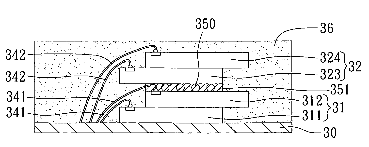
[0047]Referring to further FIG. 5, which is a schematic view of a multichip stacking structure and a fabrication method thereof according to a third preferred embodiment of the present invention. The present embodiment is similar to the foregoing embodiments except that the top chip of the first chip module of the third embodiment is electrically connected to the chip carrier by reverse wire bond technology, so as to further reduce the overall height of the stacking structure while the foregoing embodiments using a conventional wire bonding technology. The corresponding or equivalent elements in this embodiment and the forgoing embodiments will be described with the same reference numeral.
[0048]As shown in the FIG. 5, a chip 312 of a first chip module 31 is bonded to the chip carrier 30 by a reverse wire bond technology. In the reverse wire bond technology, an outer end of a bonding wire 341 connected to the chip 312 is firstly bonded to a bond pad 312a of the chip 312 to form a stu...
PUM
 Abstract
Description
Claims
Application Information
 - R&D Engineer
- R&D Manager
- IP Professional
- Industry Leading Data Capabilities
- Powerful AI technology
- Patent DNA Extraction
Browse by: Latest US Patents, China's latest patents, Technical Efficacy Thesaurus, Application Domain, Technology Topic, Popular Technical Reports.
© 2024 PatSnap. All rights reserved.Legal|Privacy policy|Modern Slavery Act Transparency Statement|Sitemap|About US| Contact US: help@patsnap.com