One Transistor DRAM Device and Method of Forming the Same

a transistor and dram technology, applied in the field of semiconductor devices, can solve the problems of fluctuation of threshold voltage, increase in difficulty level of forming capacitors having the same capacitance,

Active Publication Date: 2008-08-07
SAMSUNG ELECTRONICS CO LTD
View PDF4 Cites 144 Cited by
  • Summary
  • Abstract
  • Description
  • Claims
  • Application Information

AI Technical Summary

Problems solved by technology

The difficulty level of a process of forming capacitors having the same capacitance is increasing with the recent trend toward higher integration density of semiconductor devices.
The accumulated holes result in fluctuation of the threshold voltage.

Method used


Image

  • One Transistor DRAM Device and Method of Forming the Same
  • One Transistor DRAM Device and Method of Forming the Same
  • One Transistor DRAM Device and Method of Forming the Same

Examples


Embodiment Construction

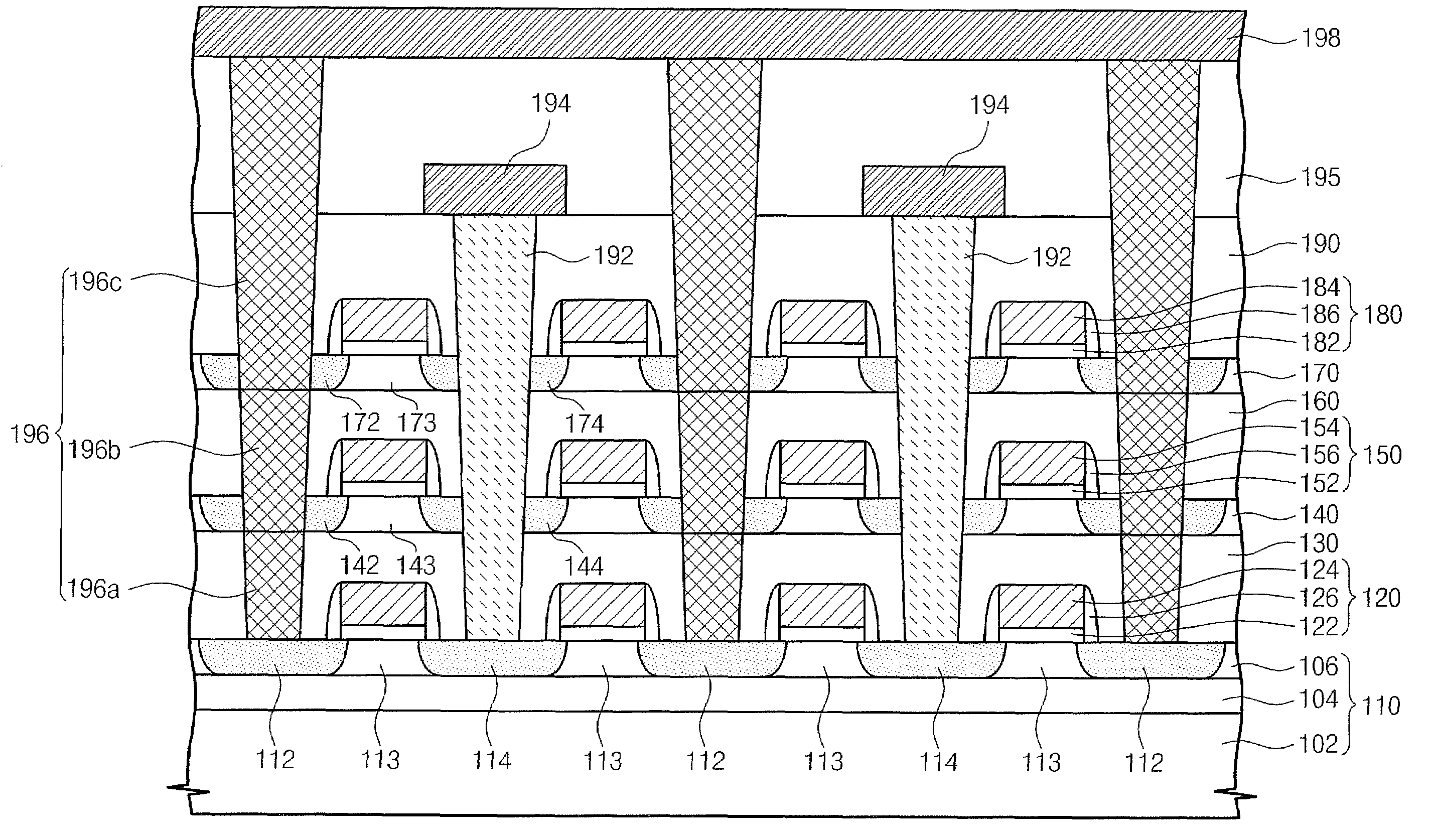
[0021]The present invention will now be described more fully hereinafter with reference to the accompanying drawings, in which preferred embodiments of the invention are shown. This invention, however, may be embodied in many different forms and should not be construed as limited to the embodiments set forth herein. Rather, these embodiments are provided so that this disclosure will be thorough and complete, and will fully convey the scope of the invention to those skilled in the art. In the drawings, the thicknesses of layers and regions are exaggerated for clarity. It will also be understood that when a layer is referred to as being “on” another layer or substrate, it can be directly on the other layer or substrate, or intervening layers may also be present. Like numbers refer to like elements throughout.

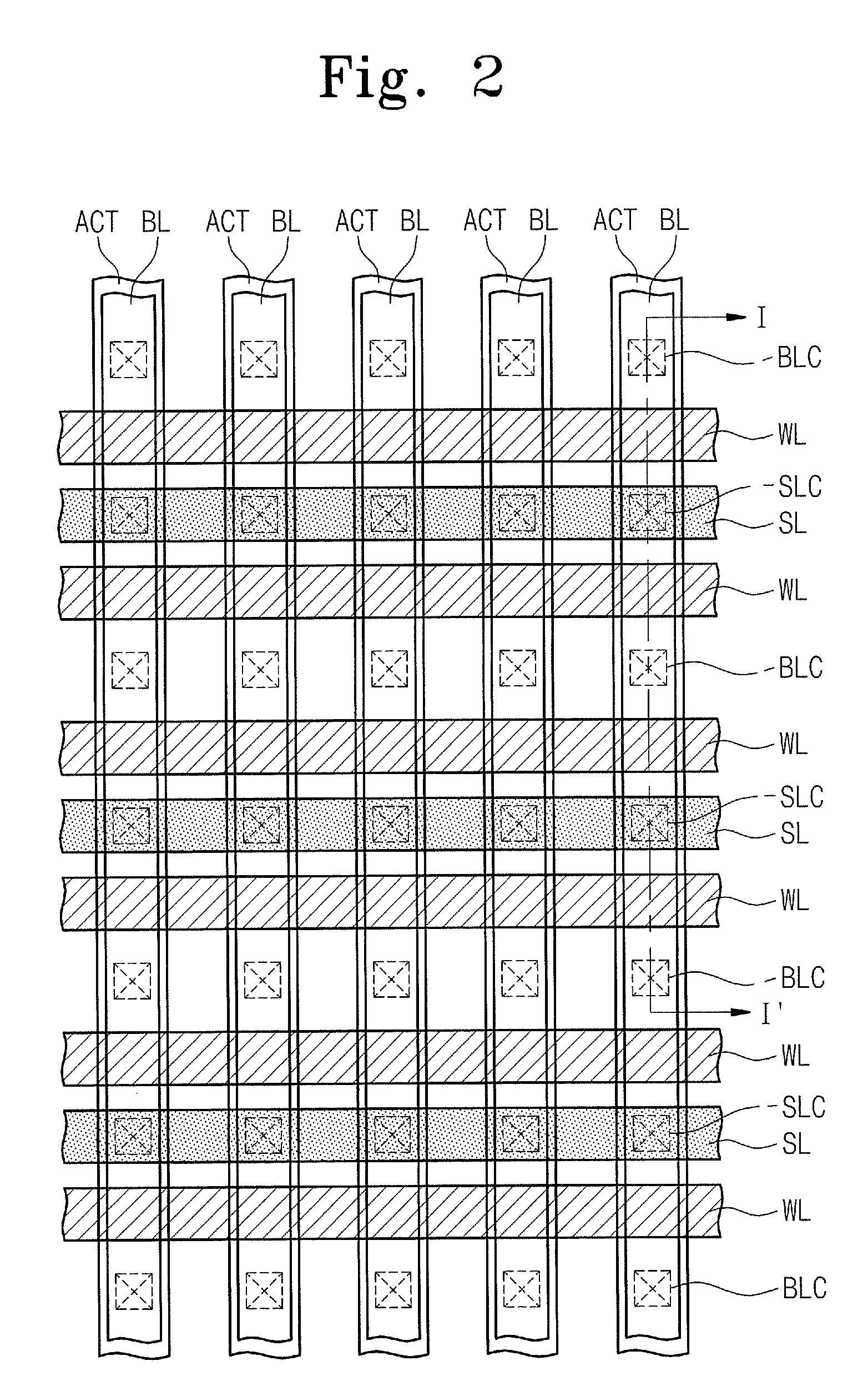
[0022]FIGS. 2 and 3 are top plan views of one transistor DRAM devices according to embodiments of the present invention, respectively. Referring to FIG. 2, active regions ACT are ...


PUM

PropertyMeasurementUnit
insulatingaaaaaaaaaa
chargeaaaaaaaaaa
electricallyaaaaaaaaaa

Abstract

A one transistor DRAM device includes: a substrate with an insulating layer, a first semiconductor layer provided on the insulating layer and including a first source region and a first region which are in contact with the insulating layer and a first floating body between the first source region and the first drain region, a first gate pattern to cover the first floating body, a first interlayer dielectric to cover the first gate pattern, a second semiconductor layer provided on the first interlayer dielectric and including a second source region and a second drain region which are in contact with the first interlayer dielectric and a second floating body between the second source region and the second drain region, and a second gate pattern to cover the second floating body.

Description

CROSS-REFERENCE TO RELATED APPLICATION[0001]This U.S. non-provisional patent application claims priority under 35 U.S.C §119 of Korean Patent Application 2007-11085 filed on Feb. 2, 2007, the entirety of which is hereby incorporated by reference.BACKGROUND[0002]The present invention relates to semiconductor devices and methods of forming the same. More specifically, the present invention is directed to a one transistor DRAM device and a method of forming the same.[0003]The semiconductor device includes a non-volatile memory such as a DRAM. Typically, a unit cell of a DRAM includes one transistor and one capacitor. The difficulty level of a process of forming capacitors having the same capacitance is increasing with the recent trend toward higher integration density of semiconductor devices.[0004]A variety of attempts have been made to overcome the increasing difficulty level of the process. One of these attempts is to develop a one transistor DRAM cell structure where there is one t...

Claims


Application Information

Patent Timeline
Patent Type & Authority Applications(United States)
IPC IPC(8): H01L27/12
CPCH01L21/8221H01L27/0688H01L27/108H01L29/7841H01L27/10844H01L27/1203H01L27/10802H10B12/20H10B12/01H10B12/00E02B5/085E03F5/14B01D35/02B01D35/16B01D29/6469
Inventor JEONG, JAE HUNKIM, KIM-NAMJUNG, SOON-MOONJANG, JAE-HOON
Owner SAMSUNG ELECTRONICS CO LTD
Why Eureka
Try Eureka