Light emitting diode

a technology of light-emitting diodes and diodes, which is applied in the direction of fixed installation, lighting and heating equipment, lighting support devices, etc., can solve the problems of poor reduced light-emitting streams, and loss of streams of light, so as to promote luminance performance of leds, reduce loss of light sources, and promote luminance performance.

Active Publication Date: 2008-08-07
LEXTAR ELECTRONICS CORP
View PDF3 Cites 10 Cited by
  • Summary
  • Abstract
  • Description
  • Claims
  • Application Information

AI Technical Summary

Benefits of technology

[0007]The primary purpose of the present invention is to provide an LED to solve problems found with the prior art to promote luminance performance of the LED by reducing loss of light source.
[0008]To achieve the purpose, an LED of the present invention is essentially comprised of a housing, one or a plurality of lead frame, one or a plurality of light-emitting chip, and packed colloid. Wherein, the lead frame is disposed in the housing; one or a plurality of pit accommodation portion to expose the lead frame is formed to the housing; multiple reflective sidewalls at various inclinations are disposed on sides of the accommodation portion; the light-emitting chip is disposed on the lead frame; streams of light emitted from the light-emitting chip travel in different directions through those reflective sidewalls to cause most of those streams of light to leave the accommodation portion for promoting luminance performance of the LED.

Problems solved by technology

Accordingly, those streams of light re-entering the first and the second sides 111, 112 can be easily reflected again into a bottom of the accommodation space 113 without effectively leaving the accommodation space 113 to result in loss of streams of light, reduced use efficiency of streams of light, and poor luminance performance of the LED.
However, both the first and the second sides disposed in the accommodation space at greater inclinations result in smaller area of the bottom of the accommodation space and larger area at an opening of the accommodation space to make it very difficult in properly locating both of the light-emitting chip and the conductor.

Method used


Image

  • Light emitting diode
  • Light emitting diode
  • Light emitting diode

Examples


Embodiment Construction

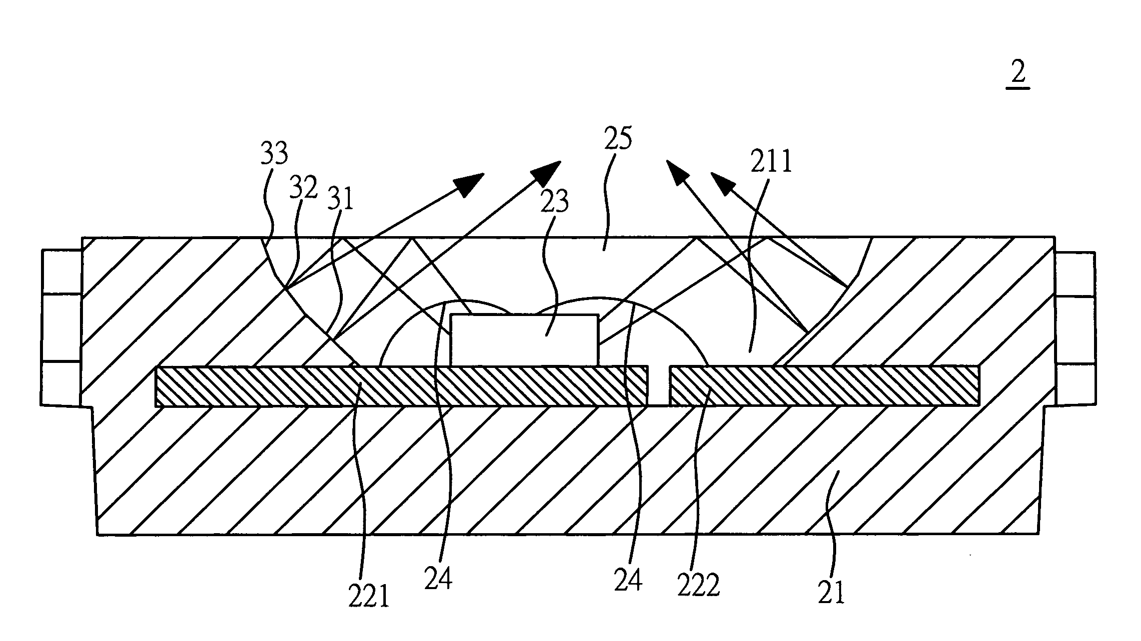
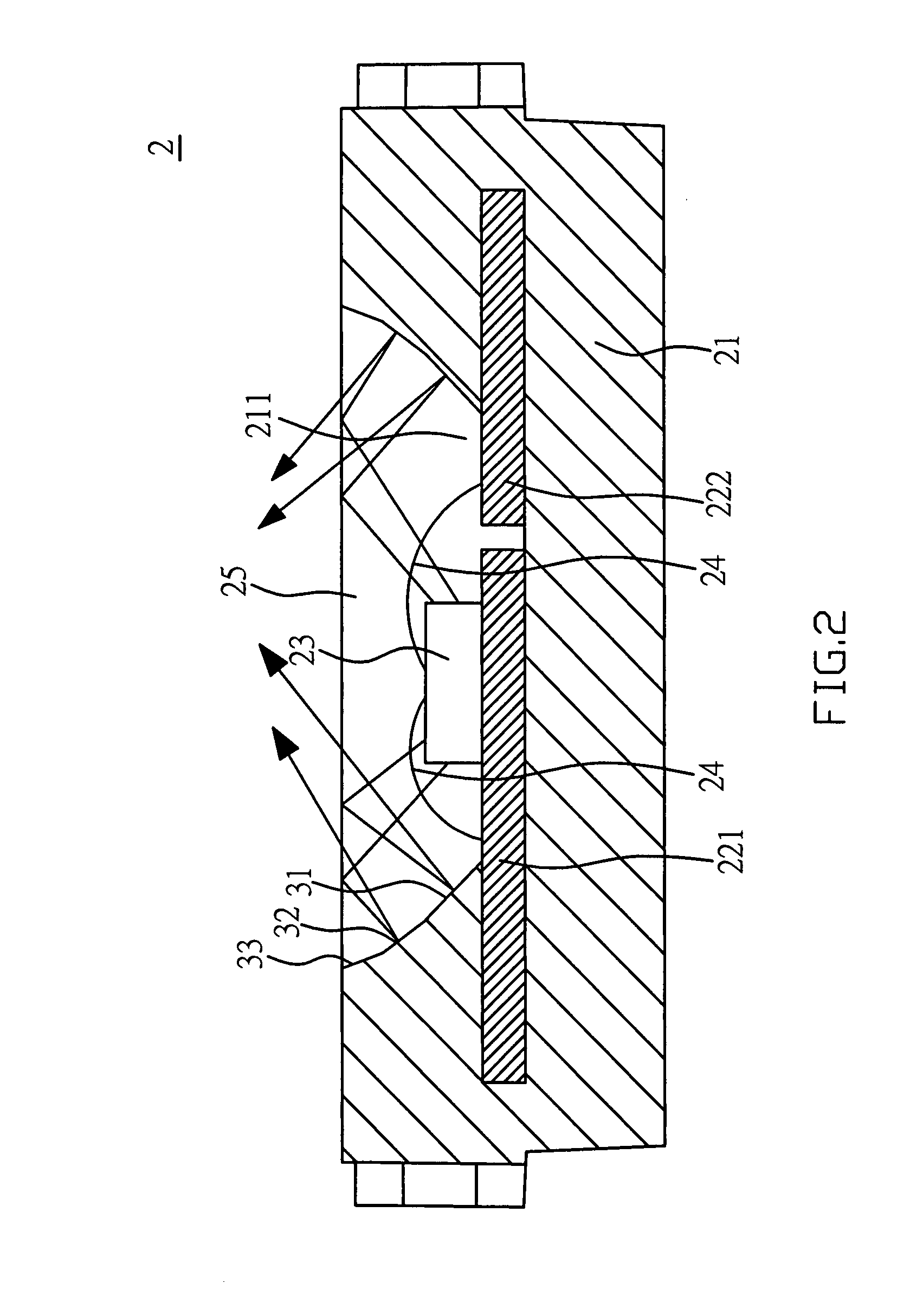
[0020]Referring to FIG. 2, an LED 2 of the present invention is essentially comprised of a housing 21, one or a plurality of light-emitting chip 23, a conductor 24, and a packed colloid 25.

[0021]The housing 21 containing two lead frames 221, 222, and a pit accommodation portion 211; both lead frames 221, 222 are partially exposed from a bottom of the accommodation portion 211; and multiple reflective sidewalls at various inclinations are disposed to multiple sides of the accommodation portion 211. As illustrated in FIG. 3, the accommodation portion 211 contains two pairs of a first and side 2111 and a second side 2112 opposite to each other; the first side 2111 is shorter than the second side 2112; and multiple, three respectively a first, a second, and a third reflective sidewalls 31, 32, 33 in the preferred embodiment as illustrated, at various inclinations are disposed to the first side 2111. As illustrated in FIG. 4, inclinations respectively of those reflective sidewalls are in...


PUM


Abstract

An LED including housing, lead frame in the housing, light-emitting chip, and packed colloid; pit accommodation portion being disposed in the housing to expose lead frame, and multiple reflective sidewalls at various inclinations being disposed on a side of accommodation portion; the chip being disposed on a lead frame; streams of light form the chip traveling in different directions when reflected by those sidewalls; and most of those streams of light being emitted out of the accommodation portion to promote luminance performance of the LED.

Description

BACKGROUND OF THE INVENTION[0001](a) Field of the Invention[0002]The present invention is related to a light emitting diode (LED), and more particularly, to one that promotes luminance performance by reducing light source loss.[0003](b) Description of the Prior Art[0004]FIG. 1 shows a schematic view of an SMD LED of the prior art, the LED 1 is comprised of a housing 11, an accommodation space 113 enclosed by a first side 111 and a second side 112 of the housing 11; a light emitting chip 12 is placed on a bottom of the accommodation space; two separately provided lead frames 13, 14 are disposed in the housing 11; the light emitting chip 12 disposed on the lead frame 13 is electrically connected to both lead frames 13, 14 respectively by means of a conductor 15; and a colloid is finally packed in the accommodation space 113 to complete a structure of the LED 1.[0005]Certain portion of streams of light emitted from the light-emitting chip 12 upon entering into where two different types...

Claims


Application Information

Patent Timeline
Patent Type & Authority Applications(United States)
IPC IPC(8): F21V7/10H01L33/48H01L33/60H01L33/62
CPCH01L33/486H01L33/60H01L2224/48091Y10S362/80H01L2924/00014
Inventor CHEN, WEI-AN
Owner LEXTAR ELECTRONICS CORP
Why Eureka
Try Eureka