AlGaInP light emitting diode

a light-emitting diode and algainp technology, applied in the field of semiconductor light-emitting diodes, can solve the problems of efficiency, and achieve the effect of improving the brightness performance of the algainp light-emitting diod

Inactive Publication Date: 2005-02-08
UNI LIGHT TECH INC
View PDF3 Cites 1 Cited by
  • Summary
  • Abstract
  • Description
  • Claims
  • Application Information

AI Technical Summary

Benefits of technology

It is an objective of the present invention to provide an AlGaInP light emitting diode, which provides an additional doped AlGaInP layer between a distributed bragg reflector and an AlGaInP illuminating layer. By way of doping the additional AlGaInP layer with a dopant concentration larger than that of an AlGaInP lower cladding layer of the AlGaInP illuminating layer or making the additional doped AlGaInP layer thicker than the AlGaInP lower cladding layer, the additional doped AlGaInP layer provides a transverse current spreading. As a result, the light-emitting region occupies the whole area of the AlGaInP light emitting diode. The brightness performance of the AlGaInP light emitting diode is thus improved.
It is another objective of the present invention to provide an AlGaInP light emitting diode, which provides an annular-shaped top electrode on a window layer thereof in order that the light emits from an AlGaInP illuminating layer would not be blocked by the top electrode. The brightness performance of the AlGaInP light emitting diode can be improved.
It is a further objective of the present invention to provide an AlGaInP light emitting diode with a light re-emitting layer including at least a first region formed of the light re-emitting layer and a second region of Al2O3 enclosing the first region. Since the refractive index of Al2O3 is much less than that of the AlGaInP illuminating layer, the light illuminating on the second region of Al2O3 from the AlGaInP illuminating layer can completely reflect back so as to improve the brightness performance of the AlGaInP light emitting diode.
In order to achieve the above objectives, the present invention provides an AlGaInP light emitting diode including a semiconductor substrate with a first conductivity, a light re-emitting layer with the first conductivity on the semiconductor substrate, an AlGaInP layer with the first conductivity and having a first doping concentration on the light re-emitting layer, an AlGaInP lower cladding layer with the first conductivity and having a second doping concentration less than the first doping concentration on the AlGaInP layer, an undoped AlGaInP active layer on the AlGaInP lower cladding layer, an AlGaInP upper cladding layer with a second conductivity opposite to the first conductivity on the undoped AlGaInP active layer, a window layer with the second conductivity on the AlGaInP upper cladding layer, an annular-shaped top electrode with the second conductivity on the window layer and a layered electrode with the first conductivity on a bottom of the semiconductor substrate. Since the doping concentration of the AlGaInP layer is larger than that of the AlGaInP lower cladding layer, the AlGaInP layer would provide a transverse current spreading. As a result, the light-emitting region occupies the whole area of the AlGaInP light emitting diode. The brightness performance of the AlGaInP light emitting diode is thus improved.

Problems solved by technology

Thus, efficiency is a very important issue.

Method used


Image

  • AlGaInP light emitting diode
  • AlGaInP light emitting diode
  • AlGaInP light emitting diode

Examples


Embodiment Construction

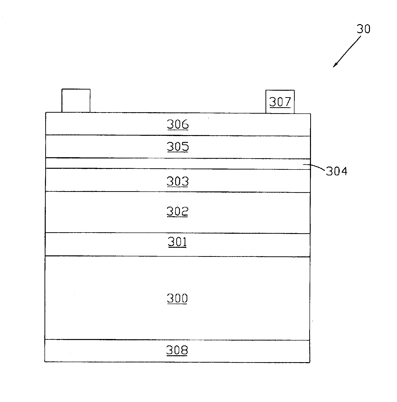
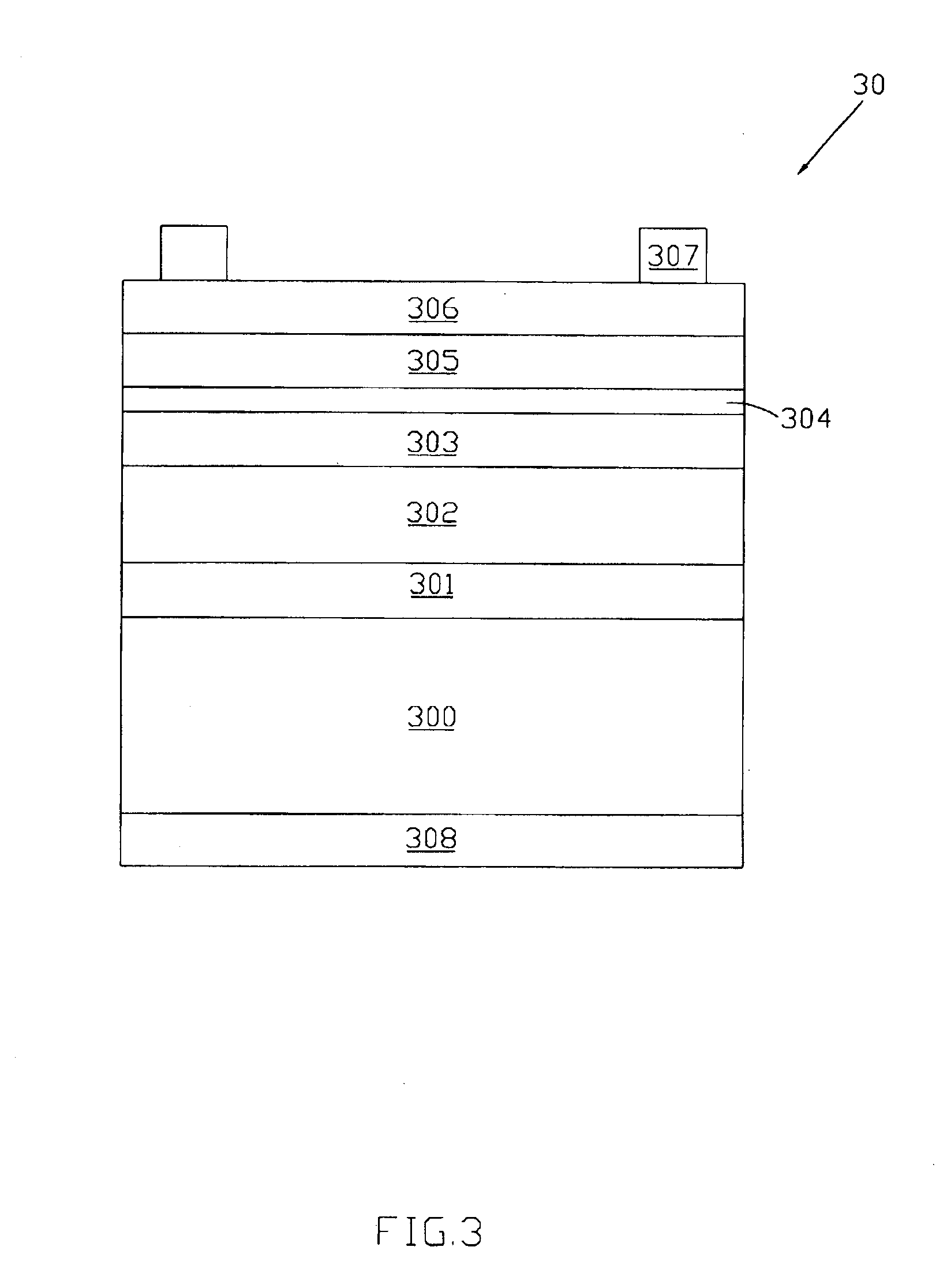
The present invention provides an AlGaInP light emitting diode with improved illumination, which forms an annular-shaped top electrode on a window layer of the AlGaInP light emitting diode such that the light emitting from the AlGaInP light emitting diode would not be blocked by the top electrode. Meanwhile, the present invention inserts an additional doped AlGaInP layer between a distributed bragg reflector and an AlGaInP illuminating layer of the AlGaInP light emitting diode. The additional doped AlGaInP layer provides a transverse current spreading so that the light-emitting region occupies the whole area of the AlGaInP illuminating layer. The illumination of the AlGaInP light emitting diode thus can be improved. The present invention also forms Al2O3 portions in the distributed bragg reflector. The refractive index of Al2O3 is about 1.55, and the refractive index of the AlGaInP illuminating layer is about 3˜3.5. The refractive index of Al2O3 is much less than that of the AlGaInP...


PUM


Abstract

An AlGaInP light emitting diode with improved illumination is provided. The AlGaInP light emitting diode includes a semiconductor substrate, a light re-emitting layer, an AlGaInP layer with a first doping concentration, an AlGaInP lower cladding layer with a second doping concentration less than the first doping concentration, an undoped AlGaInP active layer, an AlGaInP upper cladding layer, a window layer, an annular-shaped top electrode on the window layer and a layered electrode on a bottom of the semiconductor substrate. The light re-emitting layer includes at least a first region formed of the light re-emitting layer and a second region formed of Al2O3 enclosing the first region. Since AlGaInP layer between the AlGaInP lower cladding layer and the light re-emitting layer has the first doping concentration larger than that of the AlGaInP lower cladding layer, the AlGaInP layer provides a transverse current spreading. The Al2O3 region also improves light reflection illuminating on the light re-emitting layer. As a result, the brightness performance of the light emitting diode is improved.

Description

BACKGROUND OF THE INVENTION1. Field of the InventionThe present invention relates to a semiconductor light emitting diode, and more particularly to an AlGaInP light emitting diode with improved illumination.2. Description of the Prior ArtThe light emitting diode (LED) has been studied and developed for over forty years from DC 1960. From a conventional light emitting diode to a current high brightness light emitting diode, the light emitting diodes have been broadly used, such as traffic signals, car indicator lamps, colorful outside screens and even application in illumination in the future.Although the internal quantum efficiency of the light emitting diode can be improved to 90 percent and even more by the current epitaxial technique, the external quantum efficiency of the high brightness light emitting diode has an efficiency of only 10 percent or lower. Thus, efficiency is a very important issue. Improvements in the light generated within the light emitting diode and the bright...

Claims


Application Information

Patent Timeline
Patent Type & Authority Patents(United States)
IPC IPC(8): H01L33/00H01L33/10H01L33/14H01L33/30H01L33/38
CPCH01L33/10H01L33/14H01L33/30H01L33/46H01L33/387
Inventor CHEN, NAI-CHUANCHOU, YI-LUNYIH, NAE-GUANN
Owner UNI LIGHT TECH INC
Why Eureka
Try Eureka