Scanning Field Emission Display

a technology of emission display and scanning field, which is applied in the direction of discharge tube/lamp details, discharge tube main electrode, discharge tube luminescnet screen, etc., can solve the problems of arrayed field emission electron gun structurally having a problem in uniformity, fails to meet the tendency toward large-size screens, etc., and achieves low-voltage driving capability and low power consumption

Inactive Publication Date: 2008-09-04
KIM HO SEOB +1
View PDF10 Cites 5 Cited by
  • Summary
  • Abstract
  • Description
  • Claims
  • Application Information

AI Technical Summary

Benefits of technology

[0010]The multi-SFED according to the present invention overcomes disadvantages of the conventional CRT and FED and takes their advantages,

Problems solved by technology

As a result, CRT fails to meet a tendency toward the large-size screen, and undergoes a rapid drop in

Method used


Image

  • Scanning Field Emission Display
  • Scanning Field Emission Display
  • Scanning Field Emission Display

Examples


Embodiment Construction

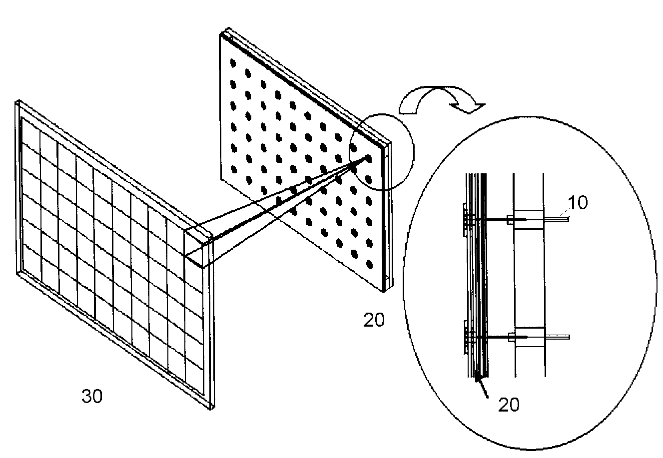
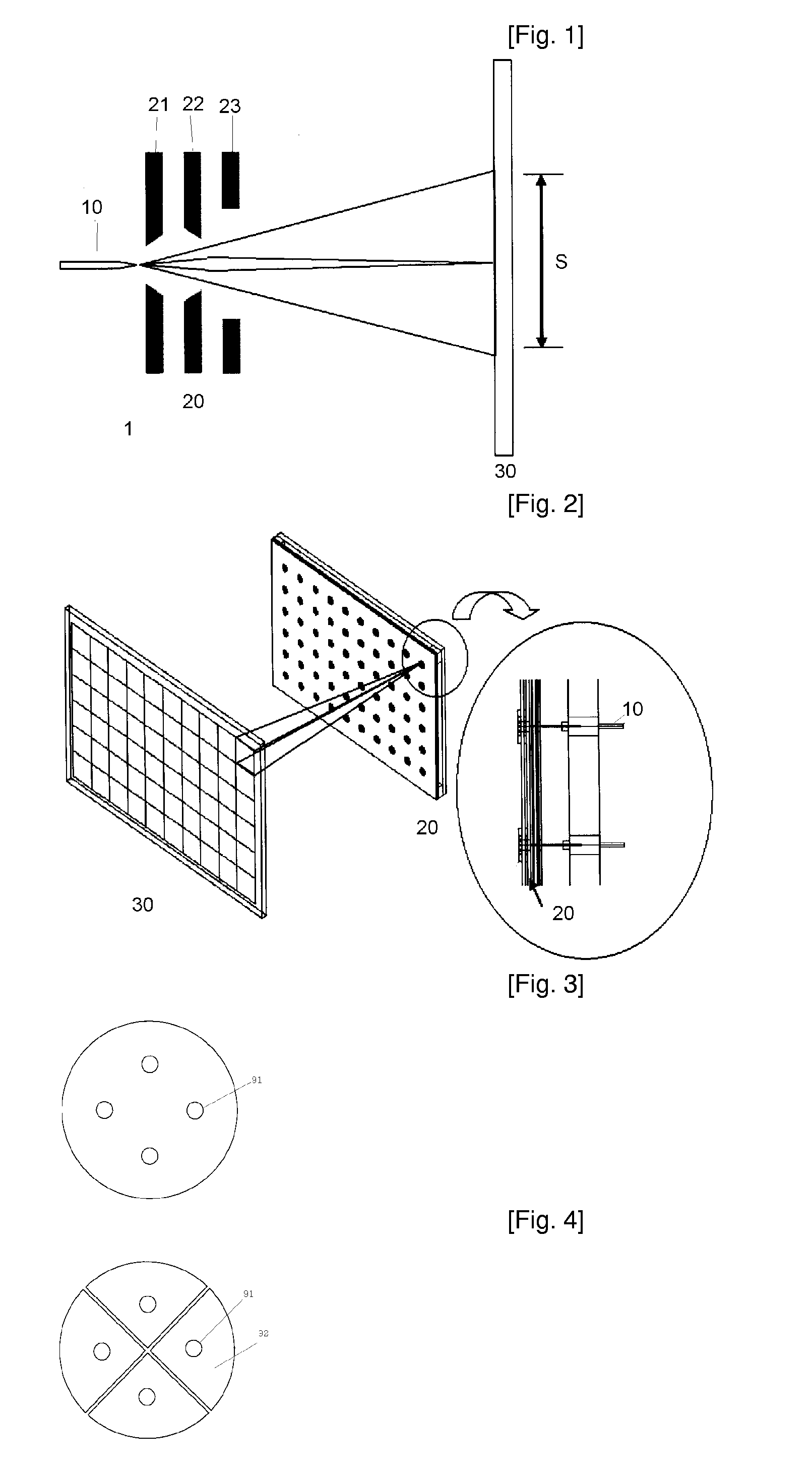
[0018]Hereinafter, a general scanning field emission display (SFED) according to the present invention will be described in detail with reference to FIG. 1. A unit SFED 1 of the present invention which electron beam scanning is possible has a basic structure of an electron emitting source 10 for emitting electrons and an SFED module 20 having an extractor 21 for extracting electron emission beam from the emitter, a control electrode 22 for accelerating and focusing the electron beam and a deflector electrode 23 for scanning the electron beam. The distance between the electron emitting source 10 and the extractor 21 is a range from tens to hundreds of micrometers. The SFED is very sensitively operated depending on characteristics of the electron emitting source 10. More particularly, the SFED are composed of the electron emitting tip 10 which is fabricated by chemically etching a tungsten wire, a source lens having the extractor 21 and control electrode 22 that bond an insulating lay...


PUM


Abstract

Provided is a scanning field emission display (SFED). The SFED includes an electron emitter and a module for inducing electron emission of the electron emitter and deflecting an electron beam. A multi-SFED may be realized as a large-sized thin and flat display by arranging in an n×m array.

Description

TECHNICAL FIELD [0001]The present invention relates to a scanning field emission display (SFED) and a multi-SFED, and more particularly to an SFED or micro CRT having a basic structure of a field emission display (FED) and scanning a predetermined domain like a CRT (Cathode Ray Tube).BACKGROUND ART [0002]CRT is basically configured of an electron gun, a deflecting yoke (or deflector) and a fluorescent screen, in which images are produced when an electron beam emitted from the electron gun is scanned on the fluorescent screen by the deflecting yoke. However, CRT dominating the display market gradually hands over its position to flat panel displays (FPDs). This is mainly responsible for the weakness of thickness, weight etc. although it is excellent in size of a screen, response speed, brightness, viewing angle, color expression etc. as compared with other displays. Thus, as the screen size increases, CRT remarkably increases in thickness and weight compared to other displays. As a re...

Claims


Application Information

Patent Timeline
IPC IPC(8): H01J1/62
CPCH01J31/127H01J1/30H01J29/52
Inventor KIM, HO SEOBKIM, BYENG JIN
Owner KIM HO SEOB
Why Eureka
Try Eureka