Scanning field emission display
A display and scanning field technology, applied in the direction of cathode ray tube/electron beam tube, discharge tube, electrical components, etc., to achieve the effect of low voltage drive capability and low power consumption
- Summary
- Abstract
- Description
- Claims
- Application Information
AI Technical Summary
Problems solved by technology
Method used
Image
Examples
Embodiment Construction
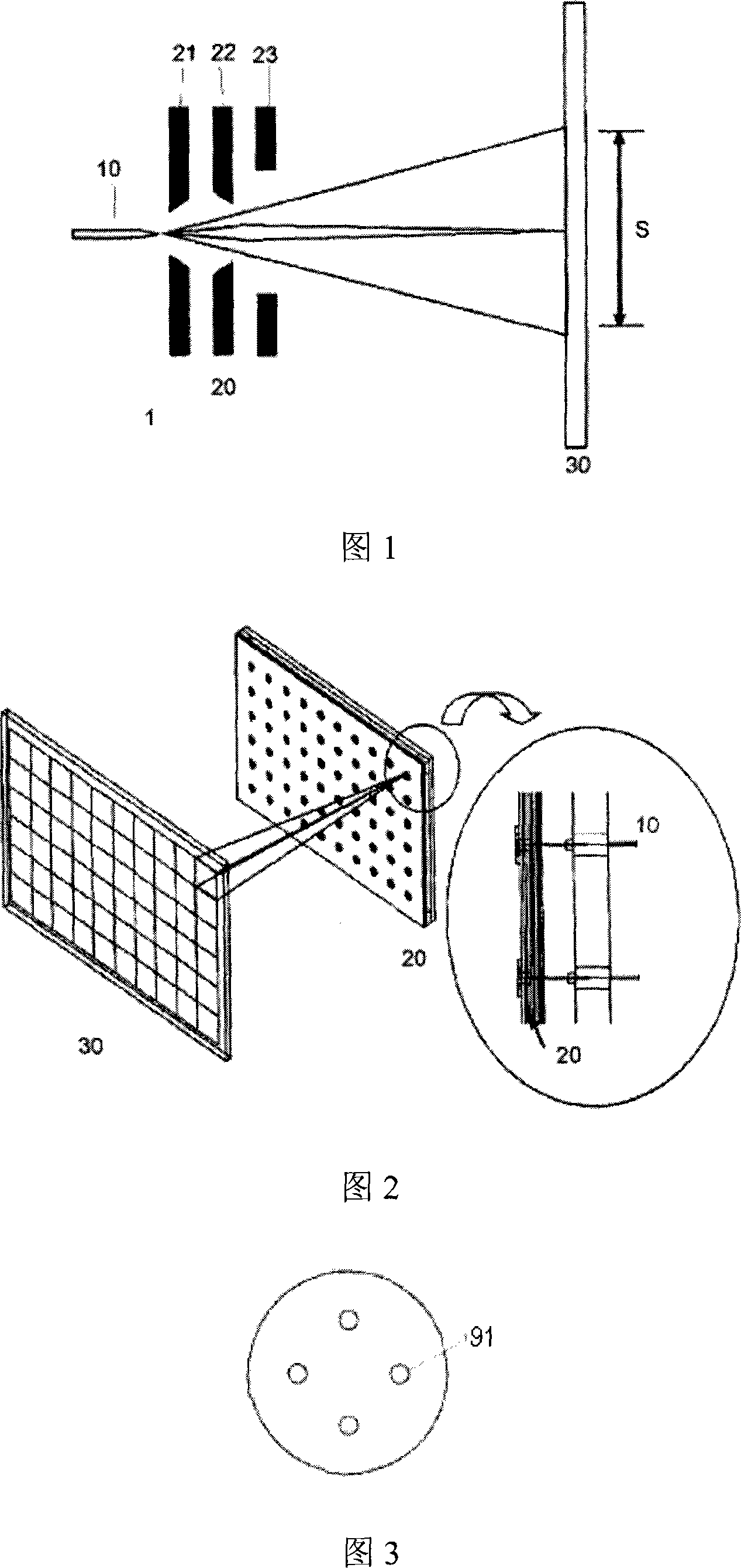
[0021] A generalized scanning field emission display (SFED) according to the present invention is described in detail below with reference to FIG. 1 . The unit SFED1 capable of electron beam scanning of the present invention has a basic structure of an electron emission source 10 for emitting electrons and an SFED module 20, and the SFED module 20 has an extractor 21 for extracting an electron emission beam from the emitter, for accelerating and A control electrode 22 for focusing the electron beam, and a deflection electrode 23 for scanning the electron beam. The distance between the electron emission source 10 and the extractor 21 is in the range of tens to hundreds of micrometers. The SFED operates sensitively depending on the characteristics of the electron emission source 10 . More specifically, the SFED includes: an electron emission tip 10 fabricated by chemically etching a tungsten wire; a source lens with an extractor 21 and a control electrode 22 bonded to an insula...
PUM
 Abstract
Description
Claims
Application Information


