
System and method for electronically combining images taken by two or more adjacent image sensors

a technology of image sensors and electronic combining, which is applied in the field of wide angle cameras, can solve the problems of long scanning time, relative short mtbf, and large size of cmos camera b>10/b> with high enough resolution, and achieves the effects of low cost, fast scanning rate and small siz

Active Publication Date: 2008-09-04
ACUANT
View PDF18 Cites 6 Cited by
  • Summary
  • Abstract
  • Description
  • Claims
  • Application Information

AI Technical Summary

Benefits of technology

[0006]In view of the limitations now present in the prior art, the present invention provides new and useful scanning devices that can maintain low cost and small size and provide for a quick scanning rate, low amortization rate and without compromising on the size of the scanned document.
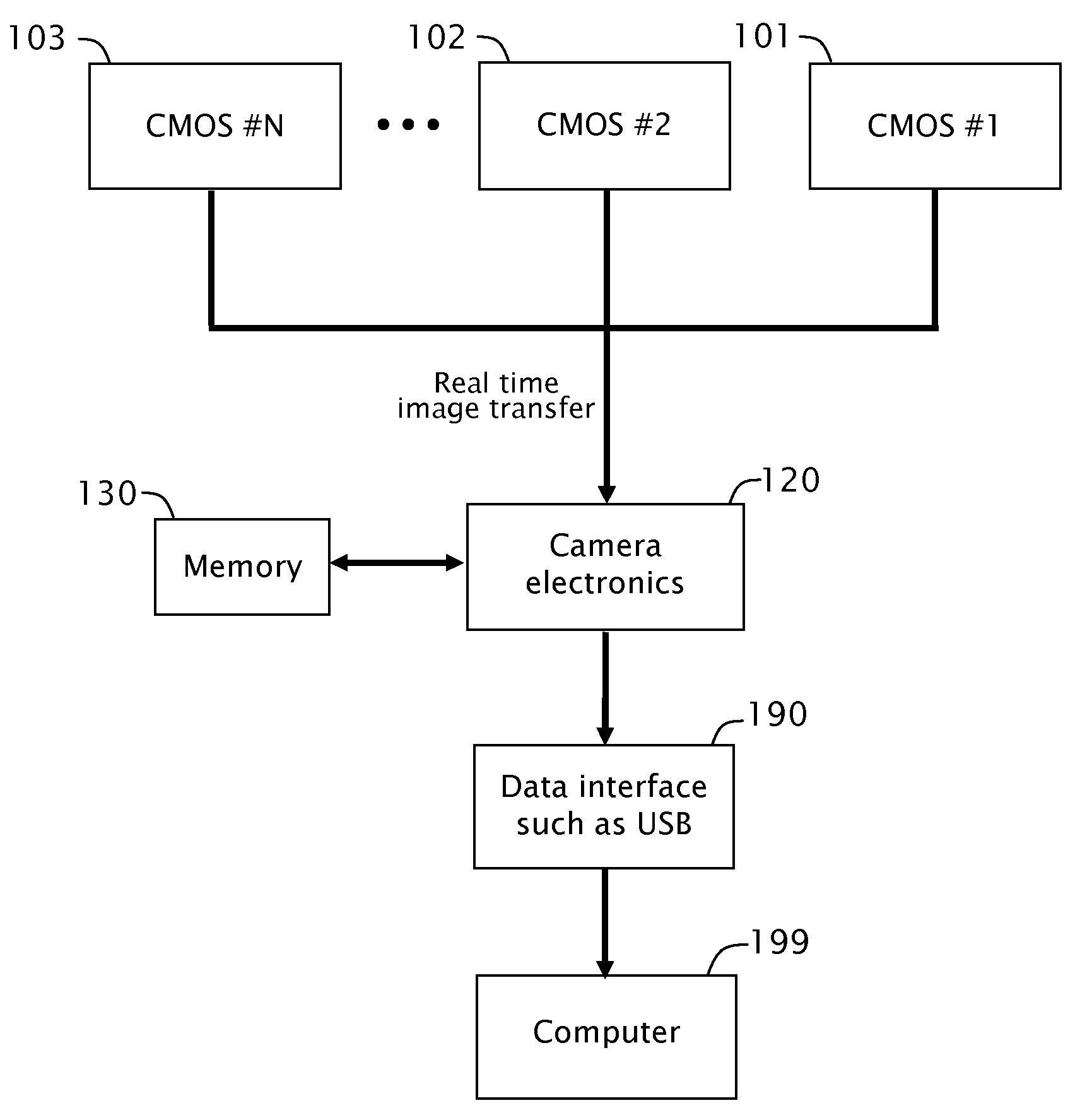
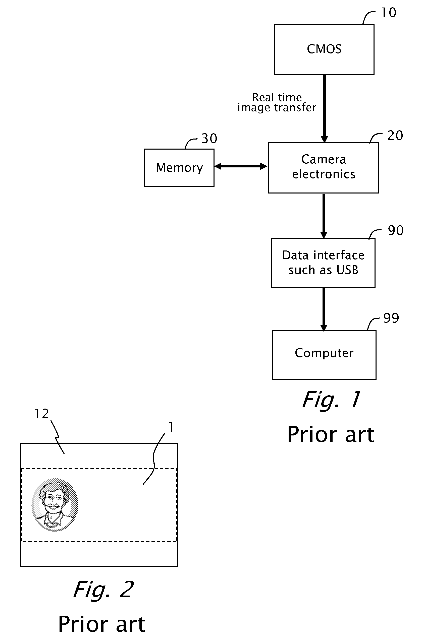
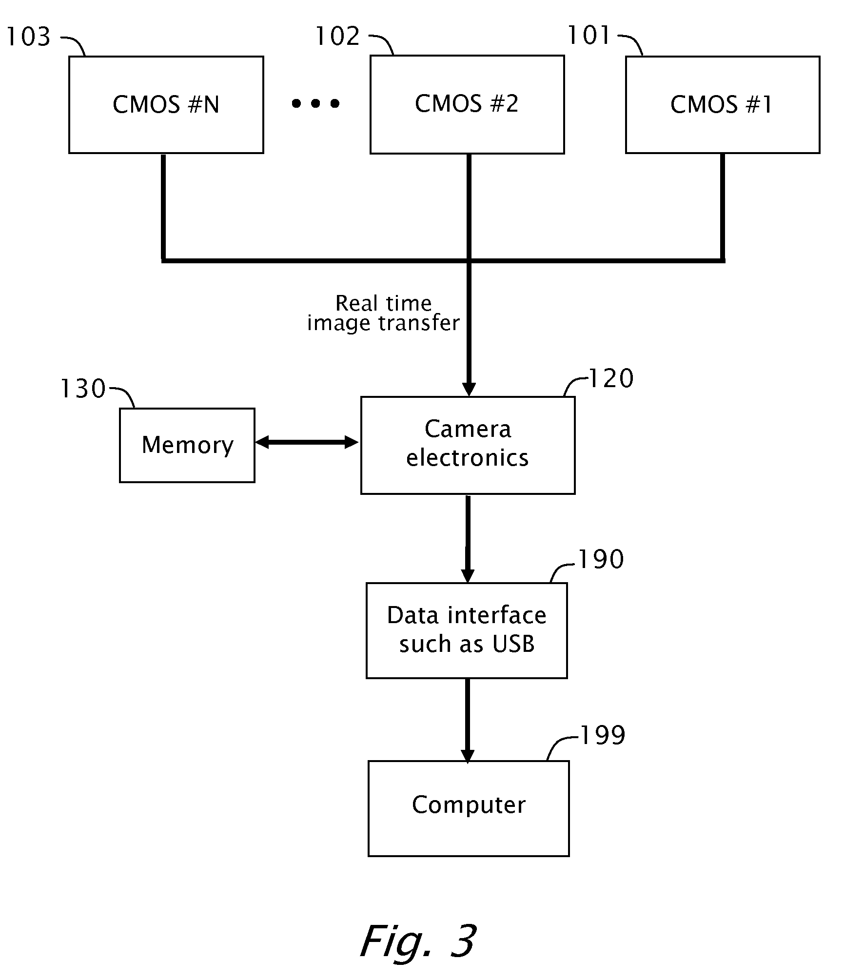
[0007]In view of the deficiencies of the prior art system illustrated in FIG. 1, the object of the present invention is then to provide a system that can use CMOS technology but still keep the size small and the cost low. Hence, the present invention provides a system that uses two or more CMOS chips, each of low cost and that acquires an image of at least part of the scanned document such that there is no gap between adjacent images but rather some overlap. Special algorithms implemented in hardware / firmware / software combination combine the images into one image of said scanned document. The image is then transferred to the computer for data extraction.
[0008]An aspect of the present invention to provide a system that can accurately align two adjacent images while correcting for radial, scale, rotation, translation and other linear or nonlinear deformations.
[0009]An aspect of the present invention to provide a system that acquires images from a closer range and with better efficiency with respect to document area coverage.
[0010]An aspect of the present invention is to provide a system capable of preventing illumination hot spots.

Problems solved by technology

On the other hand they suffer from long scanning time and a relative short MTBF due to the high amortization rate of their internal mechanisms.
But a CMOS camera 10 with high enough resolution is relative expensive and large in size.

Method used


Image

  • System and method for electronically combining images taken by two or more adjacent image sensors
  • System and method for electronically combining images taken by two or more adjacent image sensors
  • System and method for electronically combining images taken by two or more adjacent image sensors

Examples


Embodiment Construction

[0025]The present invention will now be described more fully hereinafter with reference to the accompanying drawings, in which preferred embodiments of the invention are shown. This invention may, however, be embodied in many different forms and should not be construed as limited to the embodiments set forth herein; rather, these embodiments are provided, so that this disclosure will be thorough and complete, and will fully convey the scope of the invention to those skilled in the art.

[0026]Unless otherwise defined, all technical and scientific terms used herein have the same meaning as commonly understood by one of ordinary skill in the art to which this invention belongs. The methods and examples provided herein are illustrative only and not intended to be limiting.

[0027]The main object of the present invention is then to provide new and useful scanning devices that can maintain low cost and small size and provide for a quick scanning rate and low amortization rate, and without co...


PUM


Abstract

An apparatus comprising two or more adjacent wide angle cameras, such as CMOS cameras, for imaging a document, and methods for combining corresponding images into one image while correcting radial, scale, rotation, translation and other linear or nonlinear deformations.

Description

CROSS-REFERENCE TO RELATED APPLICATIONS[0001]This application is a continuation-in-part of application Ser. No. 10 / 959,261, filed Oct. 6, 2004, which is incorporated by reference in its entirety herein. This application is related to the following U.S. patent applications:“System and method for scanning a business card from within ms outlook directly into the ms outlook contact file”, application Ser. No. 11 / 307,943 filed Feb. 28, 2006; and“System and method for creating a visitor badge for a conference or exhibition from a scanned ID or smart card document,” application No. 60 / 763,455 filed Jan. 31, 2006.The disclosures of the above applications are incorporated herein by reference.FIELD OF THE INVENTION[0002]The present invention relates to wide angle cameras, and more particularly to cameras capable of electronically combining images taken by two or more adjacent wide angle cameras.BACKGROUND OF THE INVENTION[0003]There exist in today's market scanning devices capable of reading ...

Claims


Application Information

Patent Timeline
IPC IPC(8): G06K9/00F21S6/00
CPCG03B15/00G03B27/323H04N1/19594H04N1/195G06T3/4038
Inventor HATZAV, IUVALHATZAV, DANIELBEN-SHAHAR, ILANSHARABY, GIYORA
Owner ACUANT
Learn More