Organic light emitting diode display device and method of manufacturing the same

a light-emitting diode and display device technology, applied in the manufacture of electrode systems, electric discharge tubes/lamps, discharge tubes luminescnet screens, etc., can solve the problem of uniform emission characteristics of pixels, and achieve the effect of improving mechanical reliability and preventing a voltage drop

Active Publication Date: 2008-09-11
SAMSUNG DISPLAY CO LTD
View PDF6 Cites 24 Cited by
  • Summary
  • Abstract
  • Description
  • Claims
  • Application Information

AI Technical Summary

Benefits of technology

[0011]An exemplary embodiment of the present invention provides an organic light emitting diode (OLED) display device, which includes a conductive material layer and a metal layer disposed between a cathode and an encap

Problems solved by technology

Non-uniform voltages are applied to respective pixels, theref

Method used


Image

  • Organic light emitting diode display device and method of manufacturing the same
  • Organic light emitting diode display device and method of manufacturing the same
  • Organic light emitting diode display device and method of manufacturing the same

Examples


Embodiment Construction

[0019]Reference will now be made in detail to the exemplary embodiments of the present invention, examples of which are illustrated in the accompanying drawings, wherein like reference numerals refer to the like elements throughout. The exemplary embodiments are described below, in order to explain the aspects of present invention, by referring to the figures.

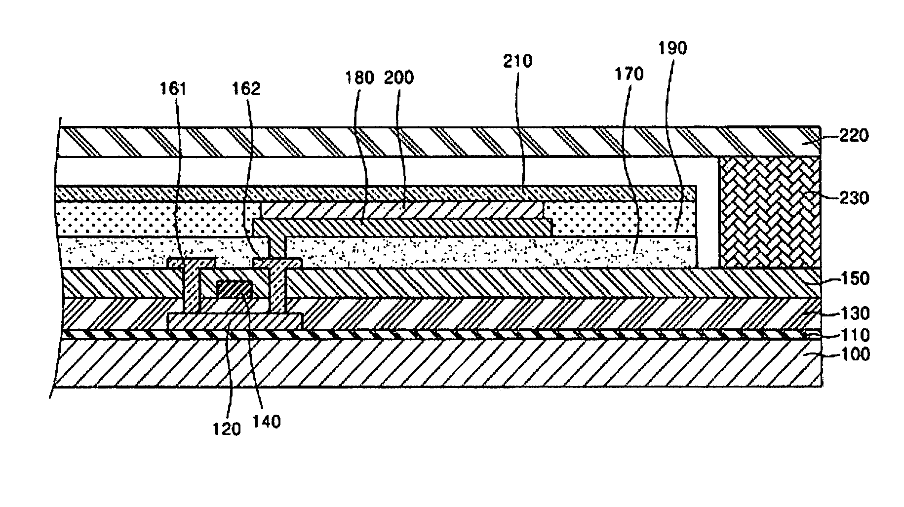
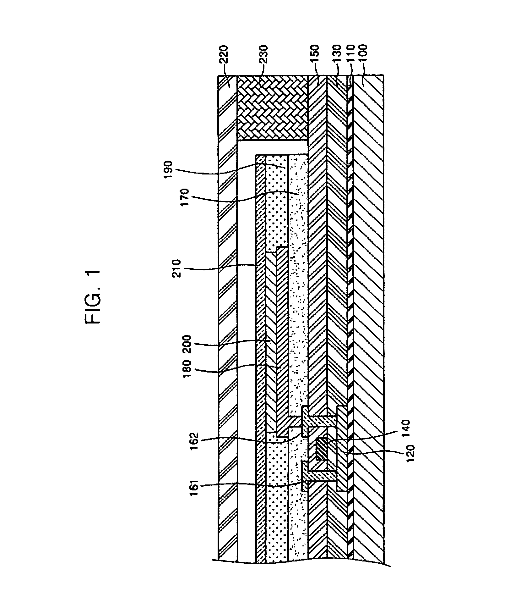
[0020]FIGS. 2 through 5 are cross-sectional views of an organic light emitting diode (OLED) display device, according to an exemplary embodiment of the present invention. As referred to herein, when a first element is said to be “disposed” or “formed” on or adjacent to a second element, the first element can directly contact the second element, or can be separated from the second element, by one or more other elements located therebetween.

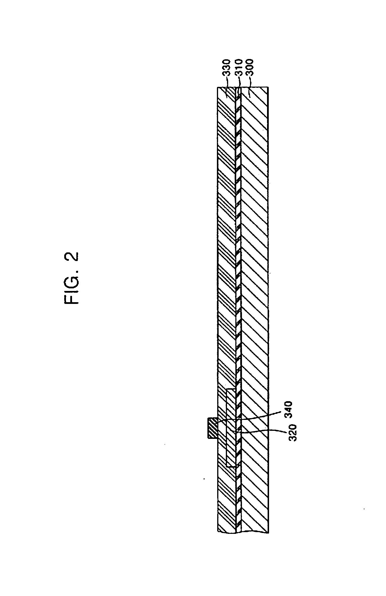
[0021]Referring to FIG. 2, a substrate 300 is provided. The substrate 300 may be an insulating glass substrate, a plastic substrate, or a conductive substrate. A buffer layer 310 is formed on ...


PUM


Abstract

An organic light emitting diode (OLED) display device, which can use a non-emission surface of an encapsulation substrate to reflect light, can prevent a voltage applied to a cathode from dropping, and has improved mechanical reliability, and a method of manufacturing the same. The OLED display device includes a substrate; a first electrode disposed on the substrate; an organic layer disposed on the first electrode; a second electrode disposed on the organic layer; a conductive material layer disposed on the second electrode; a metal layer disposed on the conductive material layer; an encapsulation substrate disposed on the metal layer; and an encapsulant to combine the substrate with an encapsulation substrate.

Description

CROSS-REFERENCE TO RELATED APPLICATION[0001]This application claims the benefit of Korean Application No. 2007-23132, filed Mar. 8, 2007, filed in the Korean Intellectual Property Office, the disclosure of which is incorporated herein by reference.BACKGROUND OF THE INVENTION[0002]1. Field of the Invention[0003]Aspects of the present invention relate to an organic light emitting diode (OLED) display device, and a method of manufacturing the same, and more particularly, to an OLED display device, which includes a conductive material layer and a metal layer disposed between a cathode and an encapsulation substrate, can prevent a voltage applied to a cathode from dropping, can reflect ambient light, and has improved mechanical reliability.[0004]2. Description of the Related Art[0005]Generally, an organic light emitting diode (OLED) display device is a self-emissive display that electrically excites organic compounds to emit light. An OLED display device may be categorized as a passive m...

Claims


Application Information

Patent Timeline
IPC IPC(8): H01L33/00
CPCH01L51/5221H01L51/5281H01L51/5237H10K50/826H10K50/841H10K50/846H10K50/86H05B33/26
Inventor KIM, EUN-AH
Owner SAMSUNG DISPLAY CO LTD
Why Eureka
Try Eureka