

Ashing method and apparatus therefor
- Summary
- Abstract
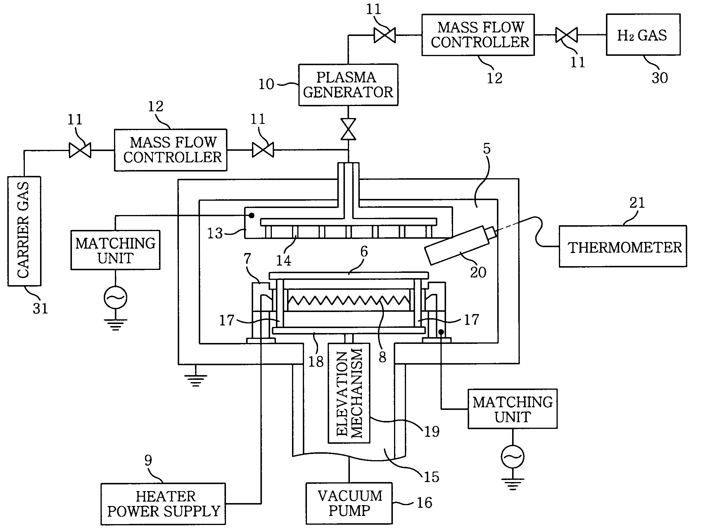
- Description
- Claims
- Application Information
AI Technical Summary
Benefits of technology
Problems solved by technology
Method used
Image

Examples
Example
Test Examples
[0058]The ashing method in accordance with the embodiment of the present invention and the conventional ashing method were respectively carried out in order to remove a plasma-etched photoresist by hydrogen radicals. Thereafter, ashing time and a generation state of a resist residue in both cases were compared.
[0059]As for a test substrate, there was used a 200 mm diameter silicon substrate on which a g-line resist is coated. The plasma etching conditions were the same as those set when the data of FIG. 3 were obtained. In the example of the present invention, a two-stage ashing process including a pre-ashing process and a main ashing process was carried out. In a comparative example, only a main ashing process was performed without a pre-ashing process.
[0060]An apparatus used herein is the same as that shown in FIG. 1. The pre-ashing process was performed in the pin up state, and the main ashing process was performed in the pin down state. Further, by using the elevati...
Example
[0062]In the ashing time, although the ashing time in the comparative example was about 190 seconds, the main ashing time in the example of the present invention was about 143 seconds, which was shortened by about 50 seconds. Therefore, it was clear that the method of the present invention can shorten the total ashing time compared to the conventional method even if the pre-ashing time of about 20 seconds is required in addition to the main ashing time.
[0063]From the above, it was found that it is possible to prevent the resist residue and shorten the ashing processing time by performing as the pre-ashing process the heating process for about 20 to 40 seconds at a temperature ranging from about 80° C. to a temperature higher than a glass transition temperature of a resist material by about 30° C.
[0064]While the invention has been shown and described with respect to the embodiments, it will be understood by those skilled in the art that various changes and modification may be made wi...
PUM
 Abstract
Description
Claims
Application Information