Light emitting device and package having the same

a technology of light emitting device and package, which is applied in the direction of semiconductor device, semiconductor/solid-state device details, electrical apparatus, etc., can solve the problems of reducing productivity, needing expensive precision processing equipment, and increasing manufacturing costs, so as to minimize reflection or absorption of emitted light, maximize luminous efficiency, and high quality

Active Publication Date: 2008-10-02
SAMSUNG ELECTRONICS CO LTD
View PDF3 Cites 93 Cited by
  • Summary
  • Abstract
  • Description
  • Claims
  • Application Information

AI Technical Summary

Benefits of technology

[0020]An aspect of the present invention provides a high quality light emitting device that can minimize reflection or absorption of emitted light, maximize luminous efficiency with the maximum light emitting area, enable uniform current spreading with a small area electrode, and enable mass production at low cost with high reliability and high quality.

Problems solved by technology

For this reason, there is a need for expensive precision processing equipment.
This causes an increase in manufacturing costs, a decrease in productivity, a decrease in yield, and a decrease in product reliability.
In general, it is difficult to form light emitting layers, which include semiconductor layers and an active layer, on the conductive substrate due to lattice-mismatching.
However, when a high-power light emitting device having a large area is manufactured, an area ratio of the electrode to the substrate needs to be high for current spreading.
Therefore, light extraction is limited, light loss is caused by optical absorption, and luminous efficiency decreases.
Further, heat, which is generated due to the absorption of the laser energy that is generally used when removing the non-conductive substrate, causes expansion and contraction of the substrate and the semiconductor layers.
Therefore, reliability of the large area light emitting device is adversely affected.

Method used


Image

  • Light emitting device and package having the same
  • Light emitting device and package having the same
  • Light emitting device and package having the same

Examples


Embodiment Construction

[0042]Exemplary embodiments of the present invention will now be described in detail with reference to the accompanying drawings. This invention may, however, be embodied in many different forms and should not be construed as limited to the embodiments set forth herein. Rather, these embodiments are provided so that this disclosure will be thorough and complete, and will fully convey the scope of the invention to those skilled in the art.

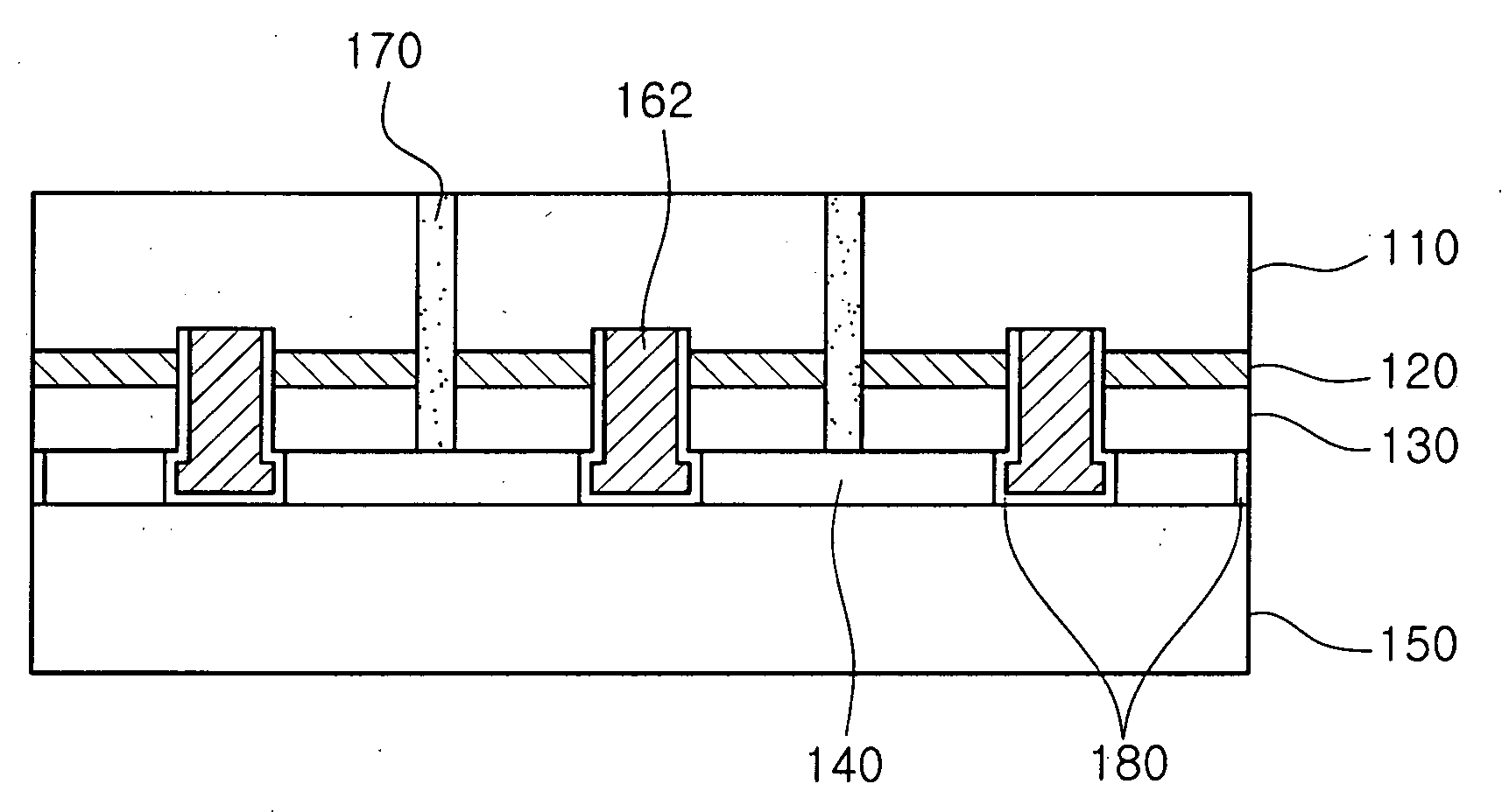
[0043]FIG. 2 is a cross-sectional view illustrating a light emitting device according to one exemplary embodiment of the present invention. FIGS. 3A and 3B are top views illustrating the light emitting device shown in FIG. 2. FIGS. 4A, 4B, and 4C are cross-sectional views illustrating the light emitting device, shown in FIG. 3B, taken along the lines A-A′, B-B′, and C-C′, respectively.

[0044]A light emitting device 100 according to the exemplary embodiment of the invention includes first and second conductivity type semiconductor layers 110 and 130, ...


PUM


Abstract

There is provided a light emitting device that can minimize reflection or absorption of emitted light, maximize luminous efficiency with the maximum light emitting area, enable uniform current spreading with a small area electrode, and enable mass production at low cost with high reliability and high quality. A light emitting device according to an aspect of the invention includes a light emitting lamination including a first conductivity type semiconductor layer, a second conductivity type semiconductor layer, and an active layer, and a conductive substrate at one surface thereof. Here, the light emitting device includes a barrier unit separating the light emitting lamination into a plurality of light emitting regions, a first electrode structure, and a second electrode structure. The first electrode structure includes a bonding unit, contact holes, and a wiring unit connecting the bonding unit to the contact holes.

Description

CROSS-REFERENCE TO RELATED APPLICATIONS[0001]This application claims the priority of Korean Patent Application No. 2007-30923 filed on Mar. 29, 2007, in the Korean Intellectual Property Office, the disclosure of which is incorporated herein by reference.BACKGROUND OF THE INVENTION[0002]1. Field of the Invention[0003]The present invention relates to a light emitting device, and more particularly, to a light emitting device that can minimize reflection or absorption of emitted light, maximize luminous efficiency with the maximum light emitting area, enable uniform current spreading with a small area electrode, and enable mass production at low cost with high reliability and high quality.[0004]2. Description of the Related Art[0005]Light emitting devices include materials that emit light. For example, light emitting diodes (LEDs) are devices that use diodes, to which semiconductors are bonded, convert energy generated by combination of electrons and holes into light, and emit light. Th...

Claims


Application Information

Patent Timeline
Patent Type & Authority Applications(United States)
IPC IPC(8): H01L33/00H01L33/08H01L33/38H01L33/62
CPCH01L33/0079H01L33/08H01L33/382H01L33/62H01L2224/32225H01L2224/48091H01L2224/48227H01L2224/48465H01L2224/73265H01L2924/00014H01L2924/01079H01L2924/00H01L33/0093
Inventor CHOI, PUN JAELEE, JIN HYUNLEE, SI HYUKMYOUNG, SEON YOUNGPARK, KI YEOL
Owner SAMSUNG ELECTRONICS CO LTD
Why Eureka
Try Eureka