Multilayer electronic component and method for manufacturing multilayer electronic component

a technology of electronic components and electronic components, applied in the direction of variable capacitors, fixed capacitor details, fixed capacitors, etc., can solve the problems of low density of plating layers formed on the surface, high manufacturing cost, and complicated process for applying catalytic metals, etc., and achieve high soldering reliability and large effective volume

Active Publication Date: 2008-10-02
MURATA MFG CO LTD
View PDF2 Cites 60 Cited by
  • Summary
  • Abstract
  • Description
  • Claims
  • Application Information

AI Technical Summary

Benefits of technology

[0016]To overcome the problems described above, preferred embodiments of the present invention provide a method for manufacturing a multilayer electronic component which includes externa

Problems solved by technology

This causes a significant increase in manufacturing cost.
A process for applying the catalytic metal is very complicated.
If no catalytic metal is applied to the surfaces, plating layers formed on the surfaces have low density, and therefore, the external electrodes have low reliability.
Therefore

Method used


Image

  • Multilayer electronic component and method for manufacturing multilayer electronic component
  • Multilayer electronic component and method for manufacturing multilayer electronic component
  • Multilayer electronic component and method for manufacturing multilayer electronic component

Examples


second preferred embodiment

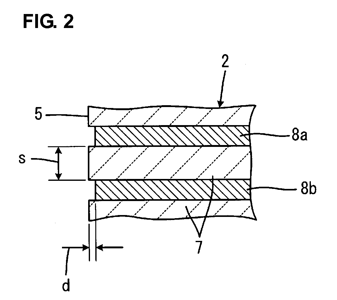
[0088]FIG. 6 shows a region near a first end surface 5 of a laminate 2 included in a multilayer electronic component 1 according to a second preferred embodiment of the present invention. FIG. 6 corresponds to FIG. 2. The same elements as those shown in FIG. 2 are designated in FIG. 6 by the same reference numerals as those shown in FIG. 2 and will not be described in detail.

[0089]In this preferred embodiment, the multilayer electronic component 1 characteristically includes first internal electrodes 8a and 8b projecting from the first end surface 5. The distance from the first end surface 5 to the top of an exposed end portion of each of the first internal electrodes 8a and 8b is herein defined as a third distance p. Where a first external electrode 10 and a second external electrode 11 are formed by electroplating, the third distance p is preferably at least about 0.1 μm. The distance between the first internal electrodes 8a and 8b adjacent to each other, that is, the first distan...

third preferred embodiment

[0096]FIG. 7 shows a region near a first end surface 5 of a laminate 2 included in a multilayer electronic component 1 according to a third preferred embodiment of the present invention. FIG. 7 corresponds to FIG. 6. The same elements as those shown in FIG. 6 are designated in FIG. 7 by the same reference numerals as those shown in FIG. 6 and will not be described in detail.

[0097]In this preferred embodiment, the multilayer electronic component 1 characteristically includes first internal electrodes 8a and 8b having projecting portions projecting from the first end surface 5. For electroplating, the distance between the first internal electrodes 8a and 8b adjacent to each other, that is, the first distance s is preferably about 20 μm or less and the distance from the first end surface 5 to the top of each projecting portion, that is, the third distance p is preferably at least about 0.1 μm. For electroless plating, the first distance s and the third distance p are preferably about 5...

fourth preferred embodiment

[0105]FIG. 8 shows a multilayer electronic component 1a according to a fourth preferred embodiment of the present invention. FIG. 8 corresponds to FIG. 1. The same members as those shown in FIG. 1 are designated in FIG. 8 by the same reference numerals as those shown in FIG. 1 and will not be described in detail.

[0106]In the multilayer electronic component 1a, after a first external electrode 10, a second external electrode 11, first thick end electrodes 14, and second thick end electrodes 15 are formed, a first plating layer 17 is formed over the first external electrode 10 and the first thick end electrodes 14 and a second plating layer 18 are formed over the second external electrode 11 and the second thick end electrodes 15 by plating.

[0107]When the first and second external electrodes 10 and 11 and the first and second thick end electrodes 14 and 15 have insufficient solder wettability, the first and second plating layers 17 and 18 are formed from a material having good solder ...


PUM

PropertyMeasurementUnit
Thicknessaaaaaaaaaa
Thicknessaaaaaaaaaa
Thicknessaaaaaaaaaa

Abstract

A method for manufacturing a laminated ceramic capacitor includes a step of preparing a laminate which has a first principal surface, a second principal surface, a first end surface, a second end surface, a first side surface, and a second side surface and which includes insulating layers and internal electrodes having end portions exposed at the first or second end surface; a step of forming external electrodes on the first and second end surfaces such that plating deposits are formed on the exposed end portions of the internal electrodes so as to be connected to each other; and a step of forming thick end electrodes electrically connected to the external electrodes such that a conductive paste is applied onto edge portions of the first and second principal surfaces and first and second side surfaces of the laminate and then baked.

Description

BACKGROUND OF THE INVENTION[0001]1. Field of the Invention[0002]The present invention relates to multilayer electronic components and methods for manufacturing the multilayer electronic components, and more particularly, to a multilayer electronic component including external electrodes formed on a laminate by plating and a method for manufacturing the multilayer electronic component.[0003]2. Description of the Related Art[0004]FIG. 9 shows a conventional multilayer electronic component 101, which is a typical laminated ceramic capacitor. The multilayer electronic component 101 usually includes a laminate 105, a first external electrode 108, and a second external electrode 109. The laminate 105 includes a plurality of insulating layers 102, a plurality of first internal electrodes 103, and a plurality of second internal electrodes 104. The first and second internal electrodes 103 and 104 are sheet-shaped and extend between the insulating layers 102. The laminate 105 has a first end ...

Claims


Application Information

Patent Timeline
IPC IPC(8): H01G4/232H01G4/30
CPCH01G4/232H01G4/30Y10T29/43Y10T29/435Y10T29/417
Inventor MOTOKI, AKIHIROKAWASAKI, KENICHIOGAWA, MAKOTOKURODA, SHIGEYUKITAKEUCHI, SHUNSUKEKASHIO, HIDEYUKI
Owner MURATA MFG CO LTD
Why Eureka
Try Eureka