Configurable pixel array system and method

Active Publication Date: 2008-11-13
SEMICON COMPONENTS IND LLC
View PDF98 Cites 193 Cited by
  • Summary
  • Abstract
  • Description
  • Claims
  • Application Information

AI Technical Summary

Problems solved by technology

However, crosstalk among pixels (e.g., light passing through a filter and striking a photosite adjacent the intended photosite) can reduc

Method used


Image

  • Configurable pixel array system and method
  • Configurable pixel array system and method
  • Configurable pixel array system and method

Examples


Embodiment Construction

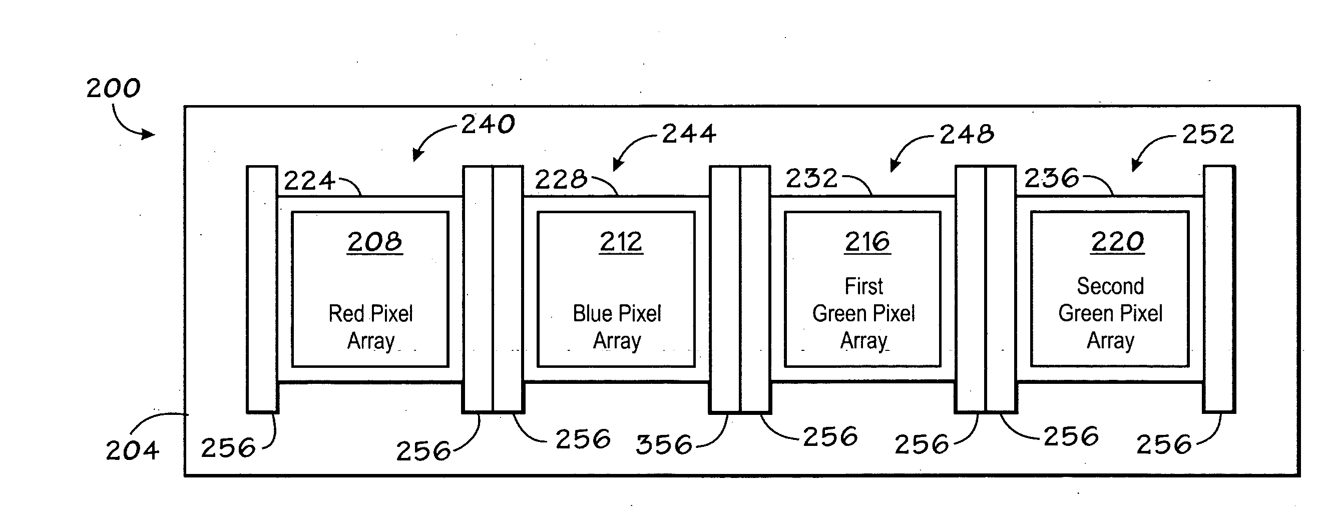
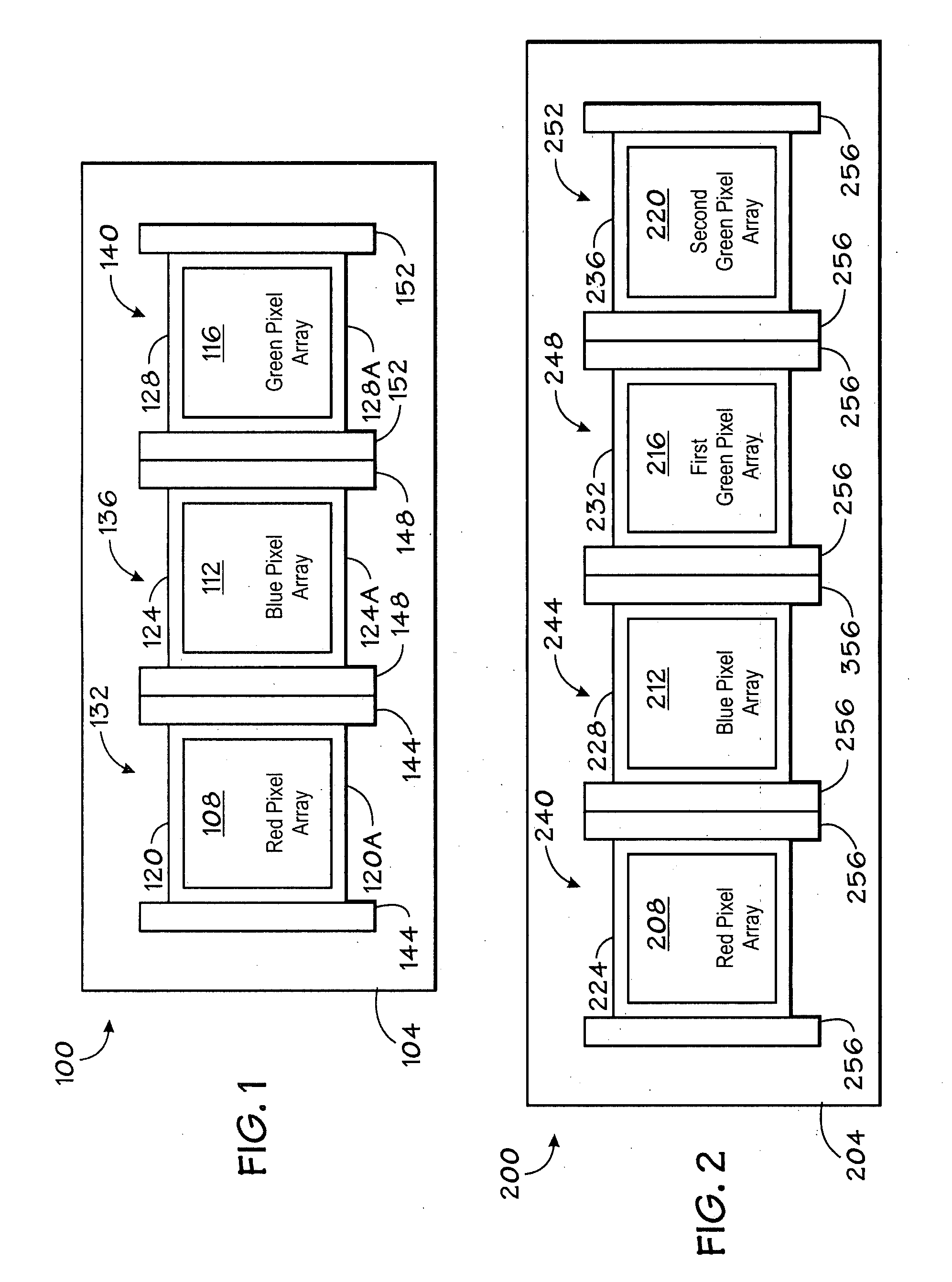
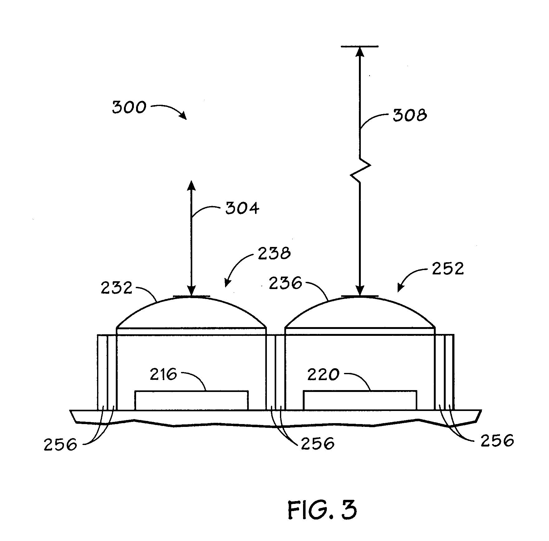
[0016]Embodiments of the present invention are directed to multi-array image sensor devices (e.g., miniaturized multi-array image sensor devices) for use in digital cameras. In contrast to traditional digital camera sensors which typically include a single monolithic array of pixels or photosites, present embodiments include flexibly sized clusters of pixels on a single die with each cluster having its own imaging lens system and / or filter above it. These arrangements of lenses, pixel clusters, and filters essentially form multiple embedded mini-cameras (i.e., small functional cameras) on each die. In accordance with present embodiments, the clusters for each mini-camera may be configured with differently sized pixels, different pixel arrangements, multiple lens types, and / or multiple color filter arrangements (e.g., a single color filter, no color filter, or a mosaic filter) based on the desired operation of the mini-camera.

[0017]Combining and integrating multiple and possibly diff...


PUM


Abstract

Present embodiments relate to techniques for capturing images. One embodiment may include an image sensor, comprising a substrate, a first pixel cell array disposed on the substrate, a first photographic lens arranged to focus light onto the first pixel cell array, a second pixel cell array disposed on the substrate, a second photographic lens arranged to focus light onto the second pixel cell array, and an image coordination circuit configured to coordinate the first array and lens with the second array and lens to provide an image. The first pixel cell array and the first photographic lens may be configured to cooperate to capture a first image of a scene, and the second pixel cell array and the second photographic lens may be configured to cooperate to capture a second image of the scene.

Description

BACKGROUND OF THE INVENTION[0001]1. Field Of The Invention[0002]The present invention relates generally to the field of semiconductor devices and more particularly to multi-array image sensor devices.[0003]2. Description of the Related Art[0004]Digital cameras, much like conventional cameras, generally include a lens or series of lenses that focus light to create an image of a target scene. The lens or series of lenses may be referred to as a photographic lens or objective lens. A photographic lens may be utilized to focus and / or magnify an image. In contrast to photographic lenses in conventional cameras, which focus light onto film, digital cameras utilize photographic lenses to focus light onto a semiconductor device that records the light electronically at individual image points (e.g., pixels or photosites). For example, instead of film, a digital camera may include a sensor (e.g., a charge coupled device (CCD) or a complementary metal oxide semiconductor (CMOS)) that converts ...

Claims


Application Information

Patent Timeline
IPC IPC(8): H04N3/14
CPCH04N5/2253H04N5/2254H04N5/2351H04N9/045H04N23/54H04N23/71H04N25/11
Inventor BOETTIGER, ULRICH C.
Owner SEMICON COMPONENTS IND LLC
Why Eureka
Try Eureka