GaN Substrate, and Epitaxial Substrate and Semiconductor Light-Emitting Device Employing the Substrate

a technology of epitaxial substrates and substrates, which is applied in the direction of semiconductor lasers, crystal growth processes, polycrystalline material growth, etc., can solve the problems of device emission efficiency degradation and emission efficiency degradation of light-emitting devices employing gan substrates, and achieve the effect of improving the emission efficiency of semiconductor light-emitting devices

Inactive Publication Date: 2008-11-20
SUMITOMO ELECTRIC IND LTD
View PDF2 Cites 192 Cited by
  • Summary
  • Abstract
  • Description
  • Claims
  • Application Information

AI Technical Summary

Benefits of technology

The patent describes new technology that helps improve how well semiconductor lights can emit light when used in the green color range. This means that these technologies are now more efficient at producing green light than they were before.

Problems solved by technology

The technical problem addressed by this patent relates to improving the emission efficiency of LEDs that use gallium nitide (GaN) substrates with traditional methods such as c-plane orientation. This method causes issues due to its polarity and results in reduced efficiencies when trying to achieve green light output from these devices.

Method used


Image

  • GaN Substrate, and Epitaxial Substrate and Semiconductor Light-Emitting Device Employing the Substrate
  • GaN Substrate, and Epitaxial Substrate and Semiconductor Light-Emitting Device Employing the Substrate
  • GaN Substrate, and Epitaxial Substrate and Semiconductor Light-Emitting Device Employing the Substrate

Examples


embodiment 1

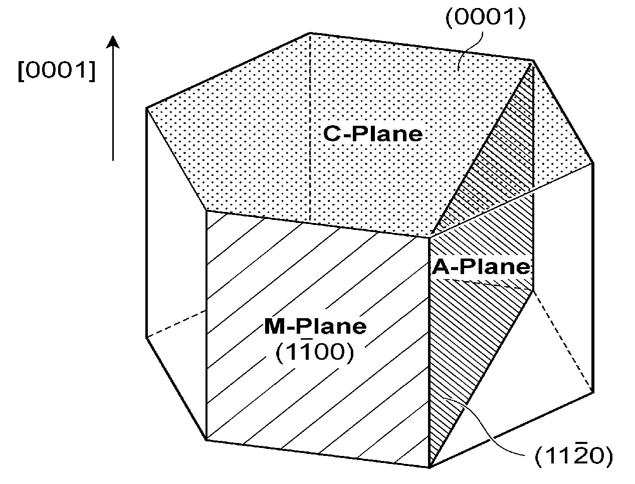
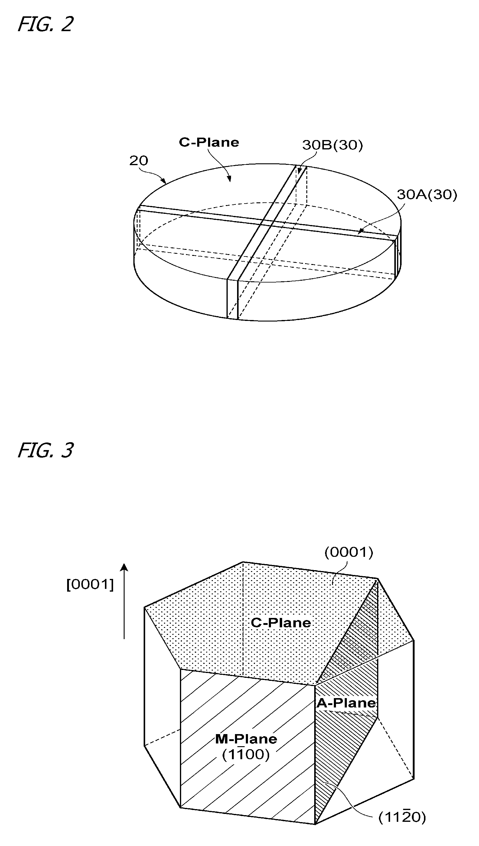
[0038]To begin with, GaN substrate Samples 1 through 14, which were the same as or equivalent to the above-described GaN substrate 30A—GaN substrates 5 mm×20 mm square, differing, as in Table I below, in off-axis angle with respect to the m-plane—were prepared according to the same procedure as that of the embodiment mode set forth above. In particular, among Samples 1-14, the misorientation axis in Samples 1-7 was a direction, and in Samples 8-14 the misorientation axis was a direction. It should be noted that the crystallographic plane orientation (off-axis angle) of the GaN substrates was characterized by x-ray diffraction, with the off-axis angle measurement accuracy being ±0.01 degrees.

TABLE IOff-axis angle0.000.030.10.30.51.02.0Sample 1Sample 2Sample 3Sample 4Sample 5Sample 6Sample 7directionSample 8Sample 9SampleSampleSampleSampleSampledirection1011121314

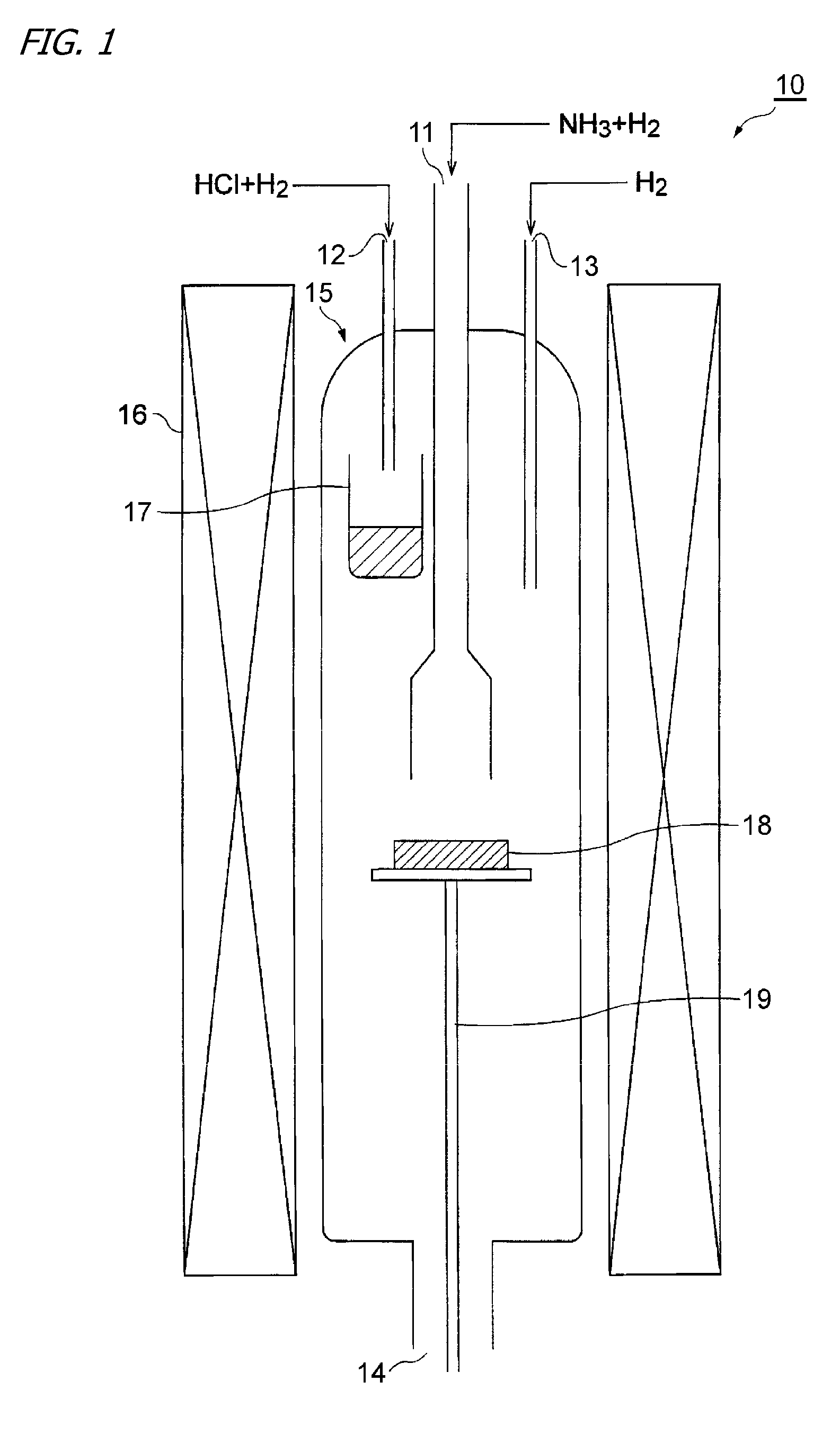
[0039]Then, an MOCVD reactor was employed to form epitaxial layers onto the growth plane of each of the above-noted Sampl...

embodiment 2

[0048]In a manner similar to that of Embodiment 1, GaN substrate Samples 15 through 28, which were the same as or equivalent to the above-described GaN substrate 30B—GaN substrates 5 mm×20 mm square, differing, as in Table IV below, in off-axis angle with respect to the a-plane—were prepared according to the same procedure as that of the embodiment mode set forth earlier. In particular, among Samples 15-28, the misorientation axis in Samples 15-21 was a direction, and in Samples 22-28 the misorientation axis was a direction. It should be noted that the crystallographic plane orientation (off-axis angle) of the GaN substrates was characterized by x-ray diffraction, with the off-axis angle measurement accuracy being ±0.01 degrees.

TABLE IVOff-axis angle0.000.030.10.30.51.02.0SampleSampleSampleSampleSampleSam-Sam-direction1516171819pleple2021SampleSampleSampleSampleSampleSam-Sam-direction2223242526pleple2728

[0049]Then, an MOCVD reactor was employed to form epitaxial layers onto the gr...


PUM


Abstract

GaN substrate (30) whose growth plane (30a) is oriented off-axis with respect to either the m-plane or the a-plane. That is, in the GaN substrate (30), the growth plane (30a) is either an m-plane or an a-plane that has been misoriented. Inasmuch as the m-plane and the a-plane are nonpolar, utilizing the GaN substrate (30) to fabricate a semiconductor light-emitting device (60) averts the influence of piezoelectric fields, making it possible to realize superior emission efficiency. Imparting to the growth plane the off-axis angle in terms of either the m-plane or the a-plane realizes high-quality morphology in crystal grown on the substrate. Utilizing the GaN substrate to fabricate semiconductor light-emitting devices enables as a result the realization of further improved emission efficiency.

Description


Claims


Application Information

Patent Timeline
Owner SUMITOMO ELECTRIC IND LTD
Why Eureka
Try Eureka