Chip-On-Lead and Lead-On-Chip Stacked Structure

a technology of lead-on-chip and stacking structure, which is applied in the direction of semiconductor devices, semiconductor/solid-state device details, electrical devices, etc., can solve the problems of chip breaking off, chip alignment is not easy, and the quantity of the package structure cannot be diminished, so as to reduce disadvantages and problems. , the effect of reducing disadvantages

Inactive Publication Date: 2008-11-20
CHIPMOS TECH INC
View PDF7 Cites 7 Cited by
  • Summary
  • Abstract
  • Description
  • Claims
  • Application Information

AI Technical Summary

Benefits of technology

[0007]In accordance with the present invention, a method and structure for packaging integrated circuits is provided which substantially eliminates or reduces disadvantages and problems associated with prior chip

Problems solved by technology

However, the lead-frame with the plurality of bending portion became deformed easily to cause the chip alignment is not easy.
In addition, the bending portion of the lead-frame would cause the inattentive of the package structure so that the quantity o

Method used


Image

  • Chip-On-Lead and Lead-On-Chip Stacked Structure
  • Chip-On-Lead and Lead-On-Chip Stacked Structure
  • Chip-On-Lead and Lead-On-Chip Stacked Structure

Examples


Embodiment Construction

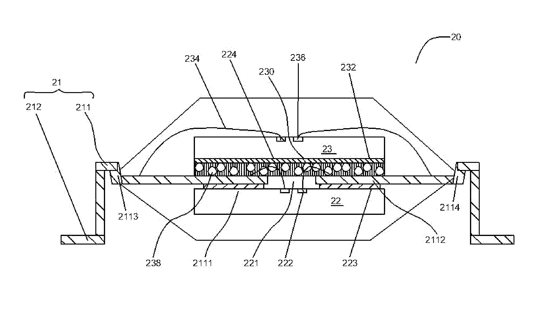
[0018]The present invention provides a method for stacking a plurality of chips with similar dimensional to form a three-dimensional package structure. In order to understand the present invention, the present invention discloses the steps of fabricating package and the structure. Obviously, the embodiment of the method of stacking chip is not limited.

[0019]The detailed description of the present invention will be discussed in the following embodiments, which are not intended to limit the scope of the present invention, but can be adapted for other applications. While drawings are illustrated in details, it is appreciated that the quantity of the disclosed components may be greater or less than that disclosed, except expressly restricting the amount of the components.

[0020]According to the semiconductor packaging process, a Front-End-Process experienced wafer is performed a thinning process firstly to reduce the thickness to a value between 2 mil and 20 mil, and then the polished wa...


PUM


Abstract

A chip-stacked package structure comprises a lead frame, a first chip, and a second chip. The led frame is composed of a plurality of inner leads and a plurality of outer leads. The plurality of inner leads comprises a plurality of first inner leads in parallel and a plurality of second inner leads in parallel, wherein the ends of first inner leads and the ends of second inner leads are arranged in rows facing each other at a distance. The active surface of first chip is fixedly connected to the lower surface of first inner leads and second inner leads via a first adhesive layer. A plurality of metal pads is provided near the central area of the active surface of first chip and is exposed. A second adhesive layer is formed on the back surface of second chip for fixedly connecting the back surface of second chip and the upper surface of first inner leads and second inner leads. The gap formed by the thickness of second adhesive layer prevents the bonding wires connecting the first chip from contacting the back surface of second chip.

Description

BACKGROUND OF THE INVENTION[0001]1. Field of the Invention[0002]The present invention provides an integrated circuit package structure and the forming method thereof, and more particular to a multichip stacked package structure of LOC (Lead on Chip) and COL (Chip on Lead).[0003]2. Description of the Prior Art[0004]In semiconductor post-processing, many efforts have been made for increasing the scale of the integrated circuits, such as memories while minimizing the occupied area. Accordingly, the development of three-dimensional (3D) packaging technology is in progress and the idea of making up a chip-stacked structure has been disclosed.[0005]In the prior, U.S. Pat. No. 6,744,121 disclosed a multi-chip package structure with a LOC lead frame as shown in FIG. 1a. Obviously, the lead-frame has a plurality of bending portion to prevent the bonding wires of the bottom chip contacting to the back surface of the upper chip. Thus, the bonding wires of the bottom chip are subjected to prote...

Claims


Application Information

Patent Timeline
IPC IPC(8): H01L23/495H01L21/98
CPCH01L23/4951H01L23/49513H01L23/49575H01L2224/32245H01L2224/48091H01L2224/48247H01L2224/73215H01L2224/73265H01L2924/01005H01L2924/01029H01L2924/01079H01L2924/01082H01L2924/14H01L2924/00014H01L24/32H01L24/48H01L2924/01033H01L24/45H01L2224/451H01L2224/45144H01L2224/45147H01L2224/4826H01L2224/48465H01L2224/8592H01L2924/181H01L2924/00H01L2224/05599H01L2924/00012H01L2224/45015H01L2924/207
Inventor CHOU, SHIH-WENPAN, YU-TANGLIN, CHUN-HUNG
Owner CHIPMOS TECH INC
Why Eureka
Try Eureka