
Method of Manufacturing Addressable and Static Electronic Displays

a static electronic display and addressable technology, applied in the field of electronic display technology, can solve the problems of complex and expensive manufacturing of lcd displays, and unsuitable for many purposes

Active Publication Date: 2008-12-04
NTHDEGREE TECH WORLDWIDE
View PDF99 Cites 80 Cited by
  • Summary
  • Abstract
  • Description
  • Claims
  • Application Information

AI Technical Summary

Benefits of technology

[0008]The exemplary embodiments of the present invention provide a new type of electronic display and a new method of manufacturing such a display, using printing and coating technologies. The inventive electronic display may be regional or static, such as for signage, or which may be addressable, such as for the display of changing information. The inventive display may be fabricated in a wide variety of sizes, from a size comparable to a mobile telephone display, to that of a billboard display (or larger). The exemplary inventive displays are also robust and capable of operating under a wide variety of conditions, including outdoor and other stressful environmental conditions.

Problems solved by technology

Such television displays have a large, very deep form factor, making them unsuitable for many purposes.
Involving myriad gas-containing and phosphor-lined cells, these displays are complicated and expensive to manufacture, also making them unsuitable for many purposes.
LCD displays also are complicated and expensive to manufacture and, again, unsuitable for many purposes.

Method used


Image

  • Method of Manufacturing Addressable and Static Electronic Displays
  • Method of Manufacturing Addressable and Static Electronic Displays
  • Method of Manufacturing Addressable and Static Electronic Displays

Examples


embodiment 185

[0104]FIG. 25 is a cross-sectional view of a sixth exemplary apparatus embodiment 185 in accordance with the teachings of the present invention. The apparatus 185 differs from the apparatus 175 insofar as the corresponding electronic components 120B are three-terminal components, such as transistors (BJTs or FETs), rather than two-terminal components (such as LEDs 120A). For such an exemplary embodiment, additional conductors are utilized, such as fourth conductors 165, with an additional insulating layer 170, as illustrated. These additional, respective conducting and insulating elements also may be formed through the printing and coating processes discussed above, as additional steps.

[0105]FIG. 26 is a cross-sectional view of a seventh exemplary apparatus embodiment 175D in accordance with the teachings of the present invention. As previously discussed, the ordering between the deposition of the plurality of first conductors 110 and the deposition of the plurality of electronic co...

embodiment 300

[0106]FIG. 29 is a block diagram illustrating a system embodiment 300 in accordance with the teachings of the present invention. The system 300 includes an apparatus 175, 185 (such as an addressable display), with the various pluralities of first conductors 110 and the plurality of transmissive second conductor(s) 140 (and the optional one or more third conductors 145) coupled through lines or connectors 310 (which may be in the form of a bus) to control bus 315, for coupling to controller (or, equivalently, control logic block) 320, and for coupling to a power source 350, which may be a DC power source (such as a battery or a photovoltaic cell) or an AC power source (such as household or building power). The controller 320 comprises a processor 325, a memory 330, and an input / output (I / O) interface 335.

[0107]A “processor”325 may be any type of controller or processor, and may be embodied as one or more processors 325, adapted to perform the functionality discussed herein. As the te...


PUM


Abstract

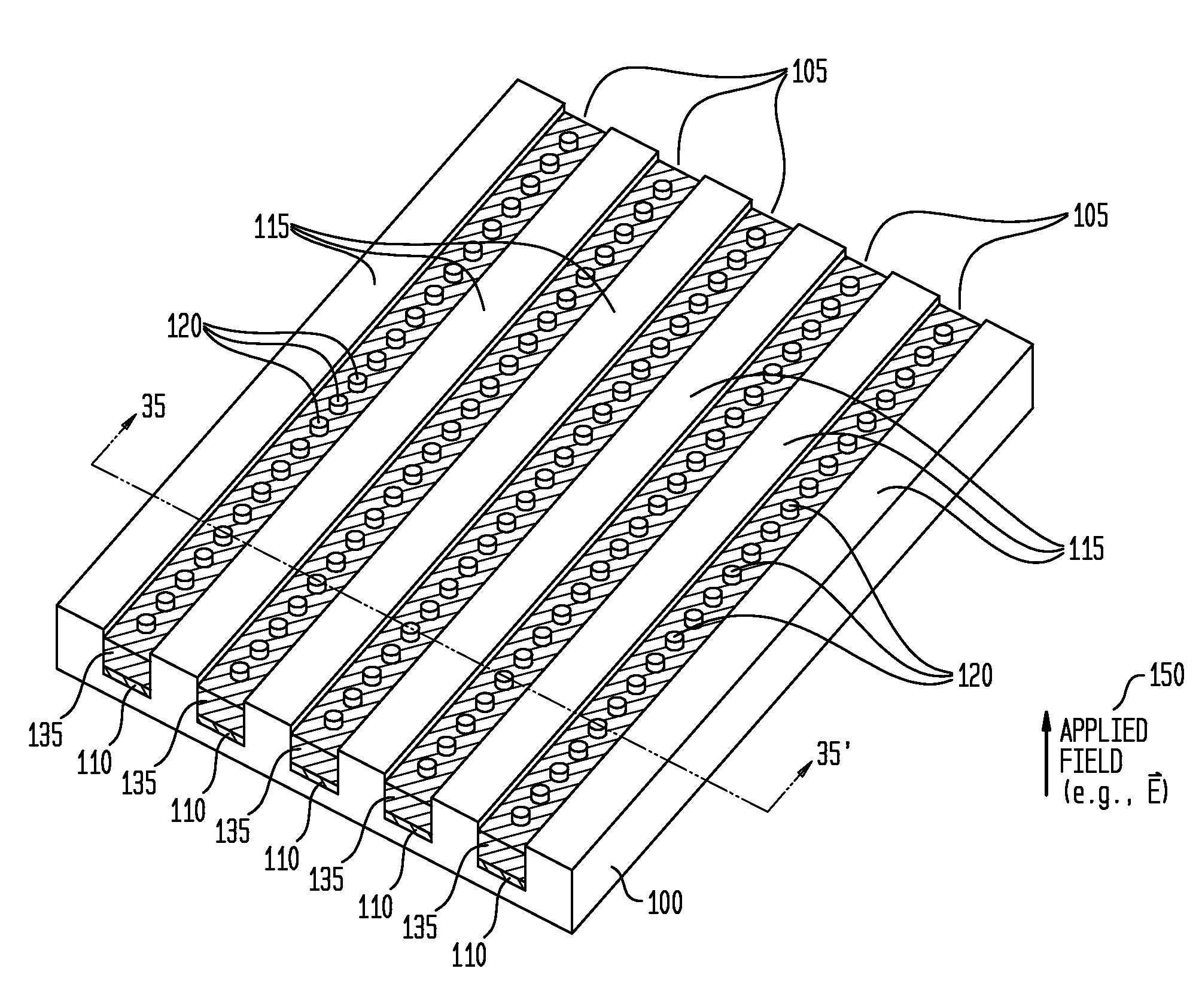
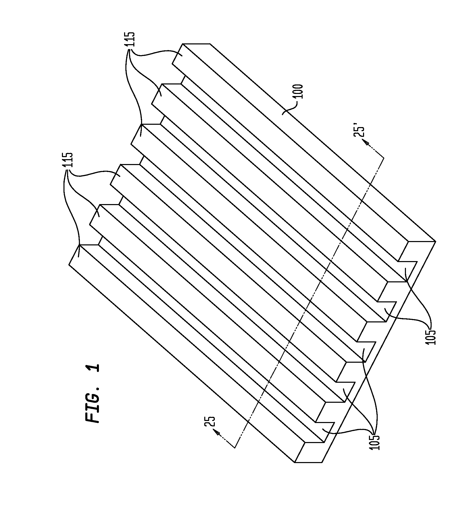
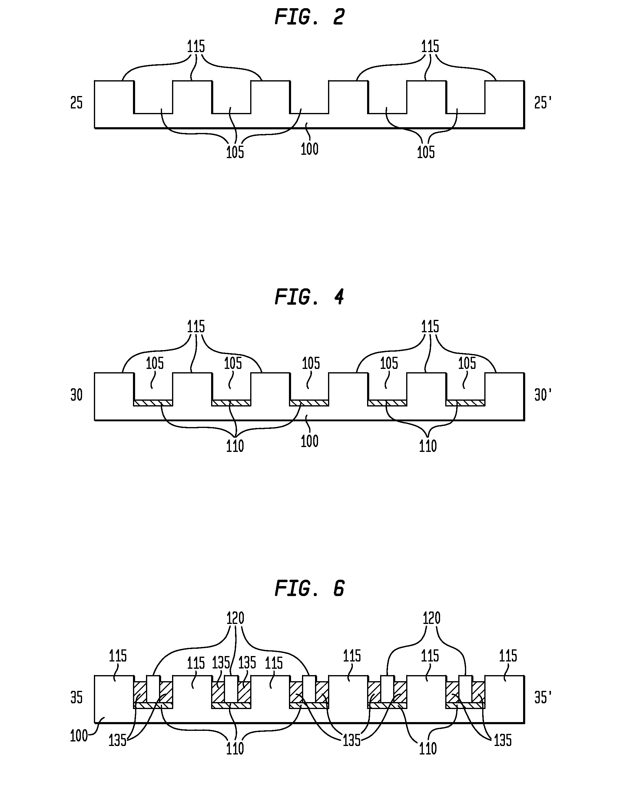
The present invention provides a method of manufacturing an electronic display. The exemplary method includes depositing a first conductive medium within a plurality of cavities of a substrate to form a plurality of first conductors. A plurality of electronic components in a suspending medium are then deposited within the plurality of cavities, and the plurality of electronic components are oriented using an applied field, followed by a bonding of the plurality of electronic components to the plurality of first conductors. A second, transmissive conductive medium is then deposited and bonded to the plurality of electronic components.

Description

FIELD OF THE INVENTION[0001]The present invention in general is related to electronic display technology and, in particular, is related to an electronic display technology capable of being printed or coated on a wide variety of substrates, and which further may be electronically addressable in various forms for real-time display of information.BACKGROUND OF THE INVENTION[0002]Display technologies have included television cathode ray tubes, plasma displays, and various forms of flat panel displays. Typical television cathode ray tube displays utilize an emissive coating, typically referred to as a “phosphor” on an interior, front surface, which is energized from a scanning electron beam, generally in a pattern referred to as a raster scan. Such television displays have a large, very deep form factor, making them unsuitable for many purposes.[0003]Other displays frequently used for television, such as plasma displays, while having a comparatively flat form factor, involve a complex ar...

Claims


Application Information

Patent Timeline
Patent Type & Authority Applications(United States)
IPC IPC(8): G09G3/32
CPCH01L27/3281H01L51/52H01L51/56H01L25/0753H01L2933/005H01L2933/0066H01L2933/0025H01L33/62H01L33/54H01L33/507H01L2933/0041H01L2924/0002H10K59/17H10K50/80H10K71/40H01L2924/00H10K71/00
Inventor RAY, WILLIAM JOHNSTONELOWENTHAL, MARK DAVID
Owner NTHDEGREE TECH WORLDWIDE
Learn More