Semiconductor device and method of fabricating the same

Inactive Publication Date: 2008-12-25
KK TOSHIBA
View PDF5 Cites 4 Cited by
  • Summary
  • Abstract
  • Description
  • Claims
  • Application Information

AI Technical Summary

Benefits of technology

[0009]Therefore, an object of the present invention is to provide a semiconductor device in which the floating gate electro

Problems solved by technology

As a result, the floating gate electrodes adjacent to each other in the predetermined direction are rendered electrically conductive, resulting in failur

Method used


Image

  • Semiconductor device and method of fabricating the same
  • Semiconductor device and method of fabricating the same
  • Semiconductor device and method of fabricating the same

Examples


Embodiment Construction

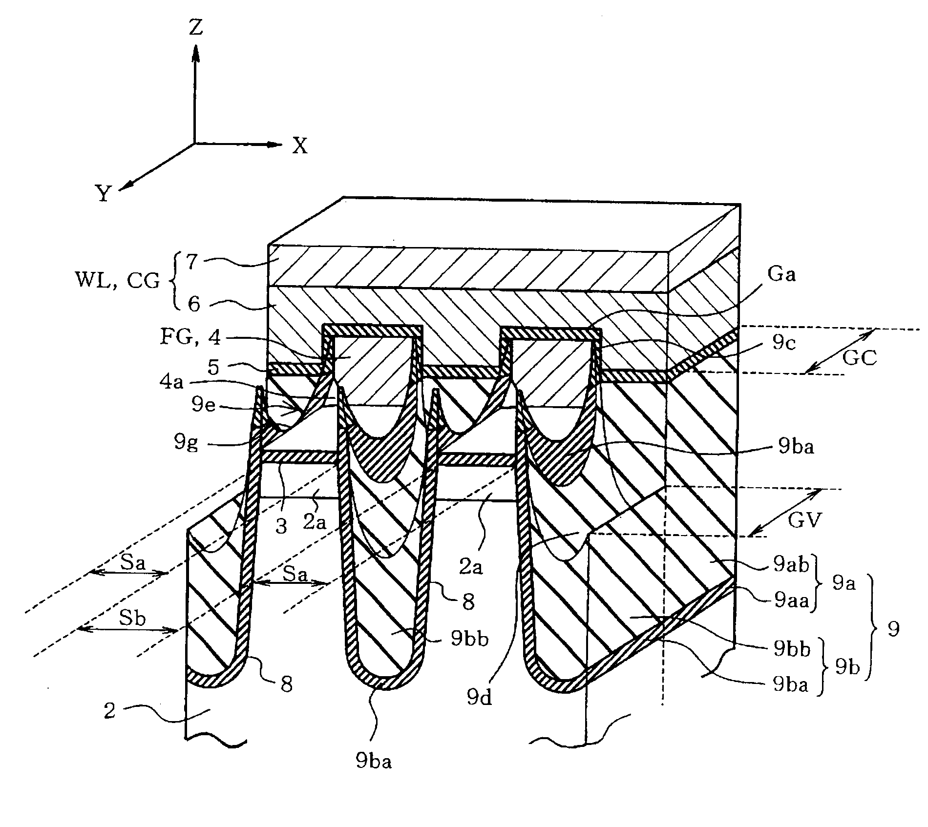
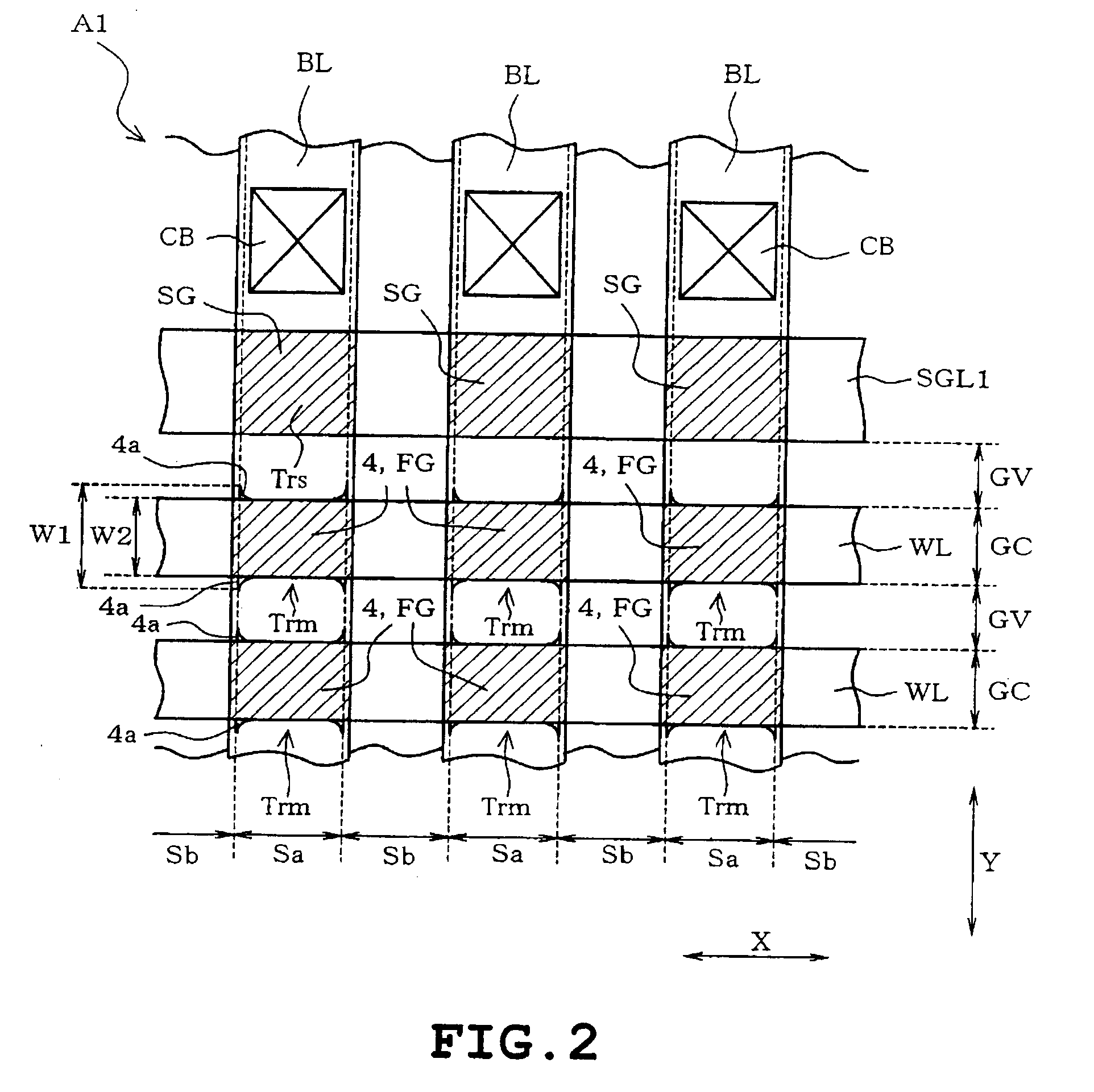
[0018]One embodiment of the present invention will be described with reference to the accompanying drawings. The invention is applied to the structure of a memory cell region of a NAND flash memory in the embodiment. Identical or similar parts are labeled by the same reference symbols throughout the figures. It is noted that the figures illustrate frame formats of the device and the relationship between a thickness and planar dimension, thickness ratio of each layer and the like differ from those of actually fabricated devices.

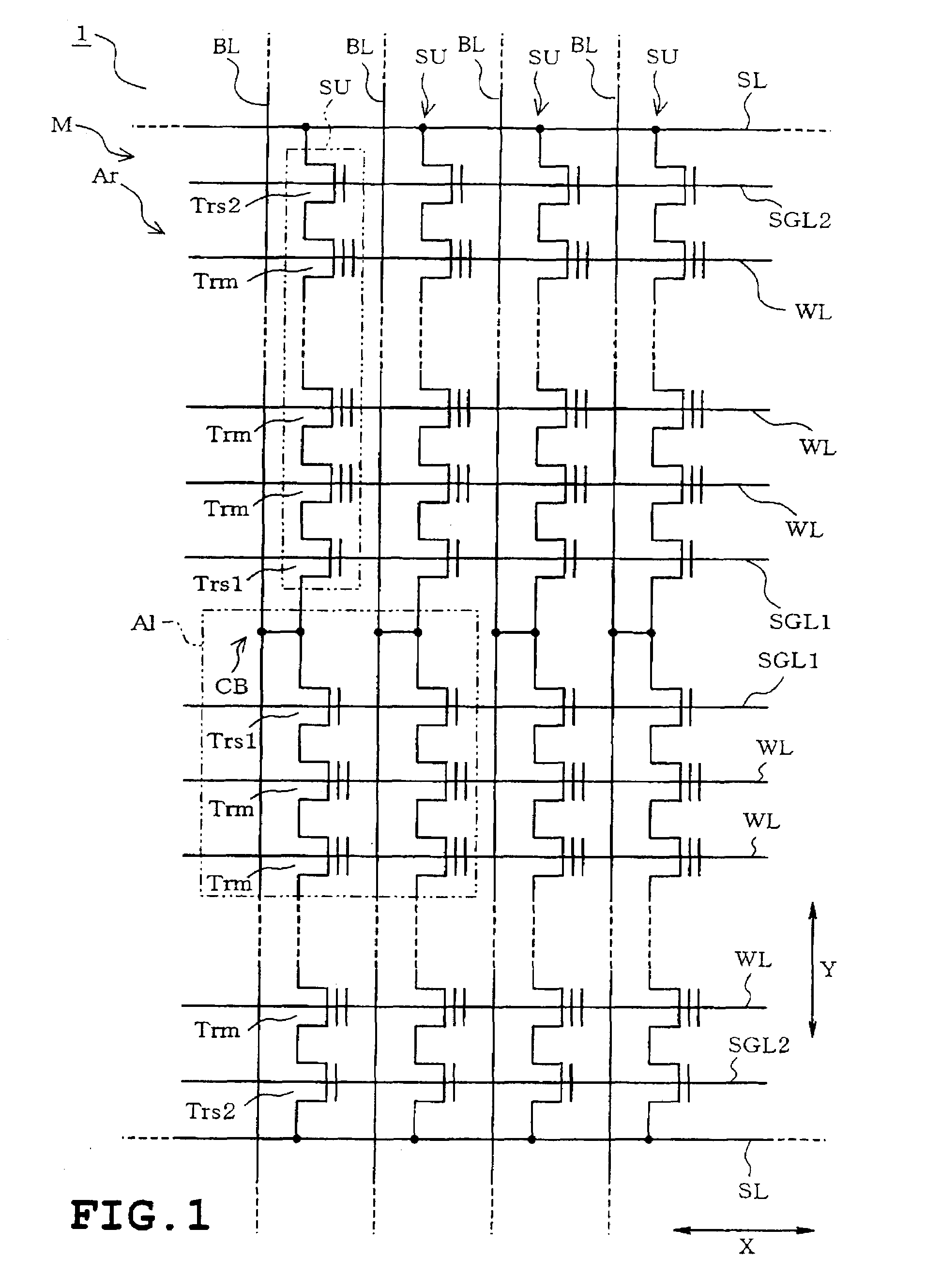
[0019]FIG. 1 is a circuit schematic equivalent to a part of memory cell array composed in a memory cell region of the NAND flash memory. As shown in FIG. 1, the NAND flash memory 1 serving as a semiconductor device includes a memory cell region M. A memory cell array Ar is configured in the memory cell region M. Each NAND cell unit comprises two selective gate transistors Trs1 and Trs2 and a plurality of memory cell transistors Trm (2n where n is a positive nu...


PUM


Abstract

A semiconductor device includes a semiconductor substrate having a plurality of element regions and a plurality of element isolation regions in a first direction, a plurality of floating gate electrodes formed via a gate insulating film on the respective element regions, an intergate insulating film formed on the floating gate electrodes, a plurality of control gate electrodes formed on the intergate insulating film so as to extend over the adjacent floating gate electrodes, and an element isolation insulating film formed in the element isolation region and having an upper end located higher than the upper surface of the gate insulating film, the element isolation insulating film including a part formed between the control gate electrodes so that the central sidewall of the element isolation insulating film is located lower than the end of the sidewall of the element isolation insulating film.

Description

CROSS-REFERENCE TO RELATED APPLICATIONS[0001]This application is based on and claims the benefit of priority from the prior Japanese Patent Application No. 2006-280184, filed on Oct. 13, 2006, the entire contents of which are incorporated herein by reference.BACKGROUND OF THE INVENTION[0002]1. Field of the Invention[0003]The present invention relates to a semiconductor device having floating gate electrodes isolated from one another by element isolation films and a method of fabricating the same.[0004]2. Description of the Related Art[0005]Fabrication of semiconductor devices such as flash memories has recently employed a process in which a gate electrode layer or floating gate electrode layer is formed prior to the forming of element isolation regions of the shallow trench isolation (STI) structure. For example, JP-A-2002-110822 discloses one of such processes in which a gate insulating film is formed on an upper surface of the semiconductor substrate. A gate electrode layer or flo...

Claims


Application Information

Patent Timeline
IPC IPC(8): H01L21/28H01L29/788
CPCH01L27/115H01L27/11521H01L29/42336H01L29/7881H10B69/00H10B41/30
Inventor MIYAZAKI, SHOICHI
Owner KK TOSHIBA
Why Eureka
Try Eureka