Electrically adjustable resistor

a technology of resistors and resistors, applied in the field of adjustable resistors, can solve the problems of not allowing significant tuning of resistance, and achieve the effect of significant tuning of resistance and enhanced vcr of polysilicon resistors

Inactive Publication Date: 2009-01-01
SEMTECH CORP
View PDF4 Cites 22 Cited by
  • Summary
  • Abstract
  • Description
  • Claims
  • Application Information

AI Technical Summary

Benefits of technology

[0011]An electrically adjustable resistor is created from a polysilicon resistive layer by taking advantage of a property of polysilicon by which the resistance changes as a function of an applied voltage. All polysilicon exhibits a voltage coefficient of resistance (VCR) that describes the small change in resistance that occurs as a result of applied voltage. A typical polysilicon resistor exhibits a VCR in the neighborhood of 1×10⁻⁴ parts per million per volt (ppm / V), which is very small and does not allow for significant tuning of the resistance. However, in accordance with the present invention, a polysilicon resistor can be deposited onto a thin dielectric layer separating the polysilicon resistor from a doped substrate acting as an adjustment layer. When a voltage is applied to the adjustment layer, the VCR of the polysilicon resistor is enhanced by over an order of magnitude, and adjustments to the voltage applied to the adjustment layer will cause the resistance of the polysilicon layer to vary with sufficient magnitude to make the device useful as an electronically tunable variable resistor.
[0012]In an embodiment of a variable resistor in accordance with the present invention, a substrate is doped with ions to create an adjustment region. A thin dielectric is deposited over the adjustment region, and two metal contacts are forced through the dielectric to make electrical contact with the adjustment region near its edges. A polysilicon layer is then deposited on top of the dielectric layer, above the adjustment region and between the metal contacts. A voltage source is connected between the metal contacts such that a voltage can be applied across the adjustment layer. The polysilicon layer can be connected to an electrical circuit to act as a resistor. When the voltage source connected between the metal contacts is varied, changing the voltage applied across the adjustment region, the resistance of the polysilicon layer changes. The precise value of the resistance of the polysilicon layer can thus be actively controlled by controlling the voltage applied across the adjustment region.
[0017]In another embodiment of an electrically adjustable resistor in accordance with the present invention, the adjustability of the polysilicon resistor is increased by including a second dielectric layer and a second adjustment layer on top of the polysilicon resistive layer. In this embodiment, the polysilicon resistor is sandwiched between two layers of dielectric with a first adjustment region below and a second adjustment layer above the resistor, enhancing the VCR. The second dielectric layer is deposited on top of the polysilicon resistive layer and may extend beyond and wrap around the polysilicon layer. Metal contacts are forced through the second dielectric layer to make electrical contact with the polysilicon resistive layer so that it can be connected to an electrical circuit. The second adjustment layer is deposited on top of the second dielectric layer, above the polysilicon layer and between the metal contacts contacting the polysilicon resistive layer. A second voltage source is connected between one edge of the second adjustment layer and its other edge in order to apply a second voltage to the second adjustment layer. Operated independently, the first voltage source and the second voltage source are used to adjust the resistance of the polysilicon adjustment layer.

Problems solved by technology

A typical polysilicon resistor exhibits a VCR in the neighborhood of 1×10⁻⁴ parts per million per volt (ppm / V), which is very small and does not allow for significant tuning of the resistance.

Method used


Image

  • Electrically adjustable resistor
  • Electrically adjustable resistor
  • Electrically adjustable resistor

Examples


Embodiment Construction

[0027]The present invention satisfies the need for an improved and cost-effective way of adjusting resistance values in polysilicon resistors.

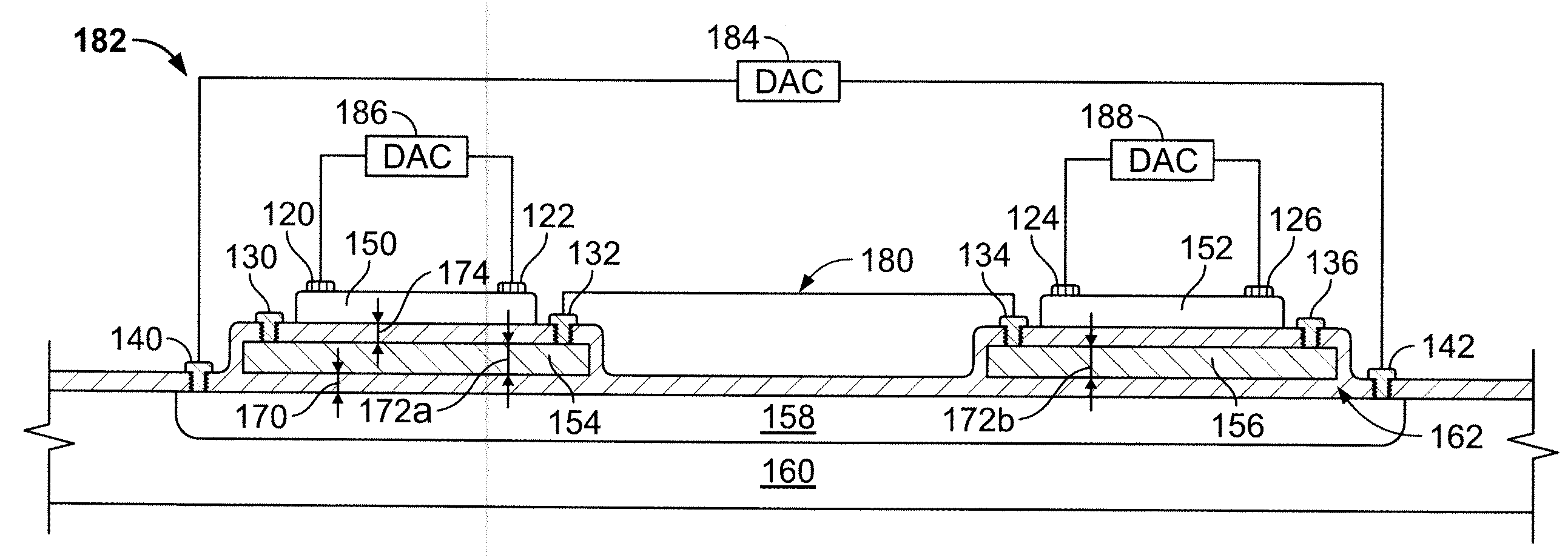
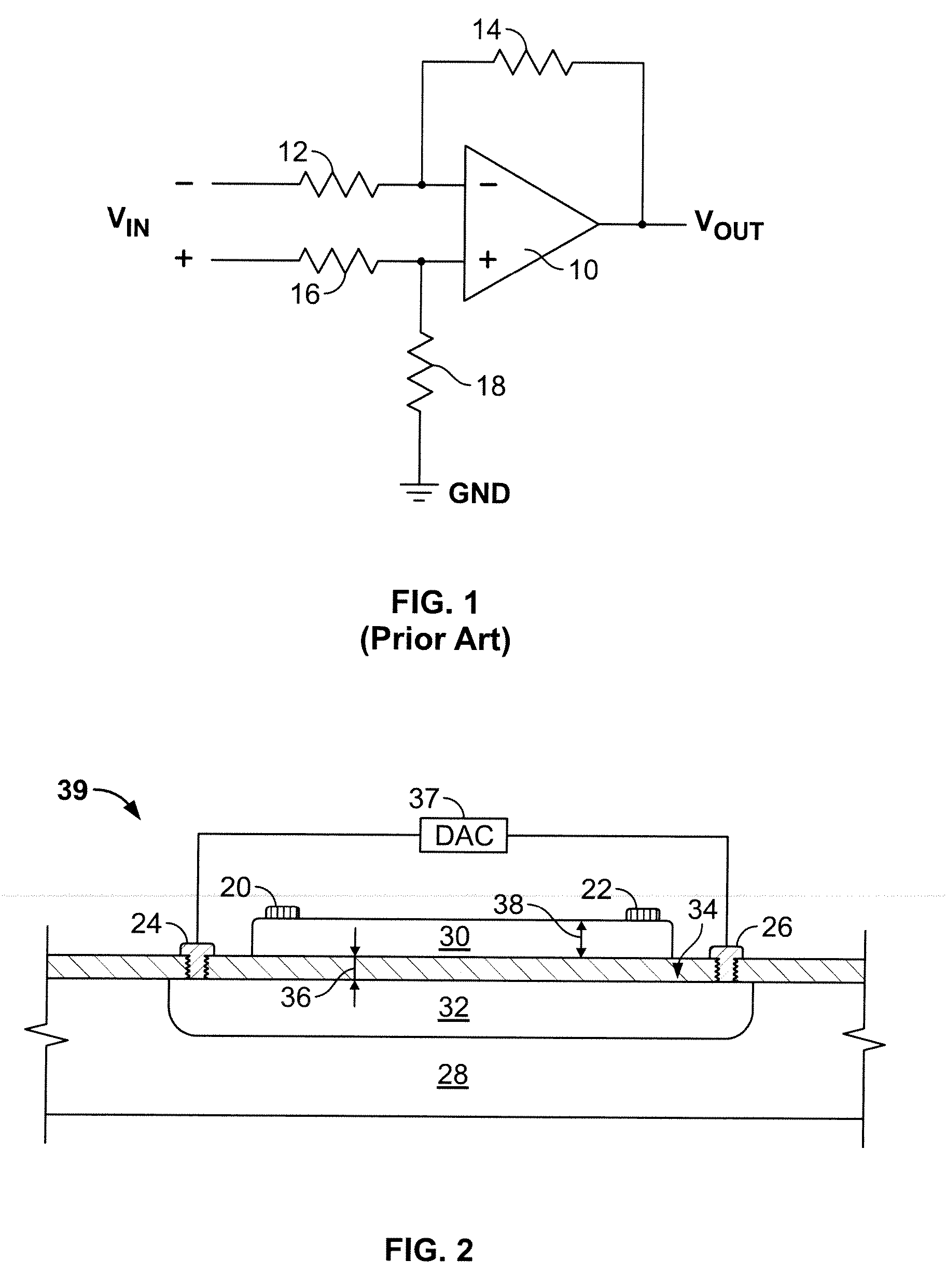
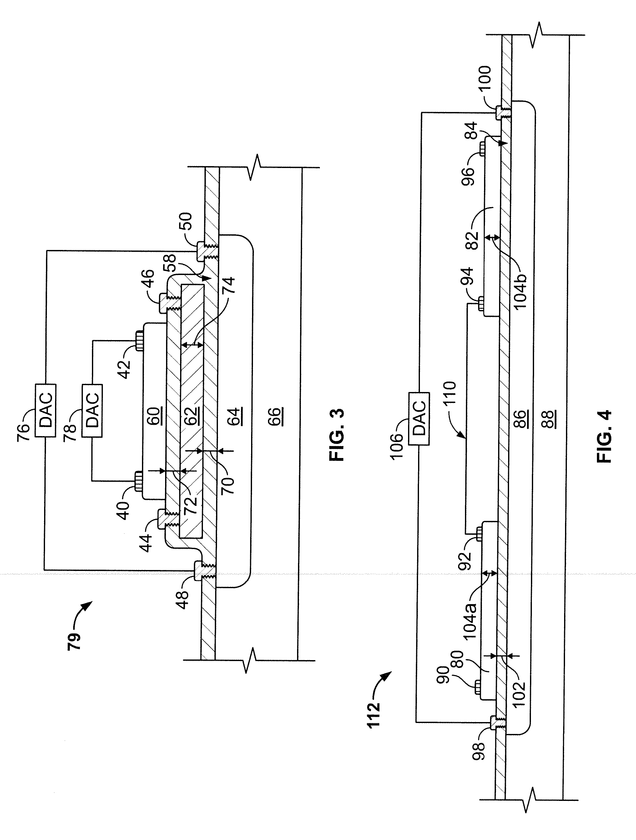
[0028]FIG. 2 provides a cross-sectional view of an electrically adjustable resistor in accordance with a preferred embodiment of the invention. The electrically adjustable resistor 39 comprises four regions: substrate 28, adjustment layer 32, polysilicon resistor layer 30, and dielectric 34. The substrate 28 forms the base on which additional materials and layers can be added. Substrate 28 can be made of either an n-substrate or a p-substrate. Ions are implanted into the substrate 28 to form the adjustment layer 32, which is an isolated p-well or n-well, depending on whether the substrate 28 is an n-substrate or a p-substrate. If an n-substrate is used, then the adjustment layer 32 will be an isolated p-well. If a p-substrate is used, then the adjustment layer 32 will be an isolated n-well. Dielectric layer 34 is formed atop adjustment layer 3...


PUM

PropertyMeasurementUnit
thicknessaaaaaaaaaa
thicknessaaaaaaaaaa
thicknessaaaaaaaaaa

Abstract

An electrically adjustable resistor comprises a resistive polysilicon layer dielectrically isolated from one or more doped semiconducting layers. A tunable voltage is applied to the doped semiconducting layers, causing the resistance of the polysilicon layer to vary. Multiple matched electrically adjustable resistors may be fabricated on a single substrate, tuned by a single, shared doped semiconductor layer, creating matched, tunable resistor pairs that are particularly useful for differential amplifier applications. Multiple, independently adjustable resistors may also be fabricated on a common substrate.

Description

RELATED APPLICATION DATA[0001]This application claims the benefit, pursuant to 35 U.S.C. § 119(e), of U.S. provisional application Ser. No. 60 / 947,372, filed Jun. 29, 2007.BACKGROUND OF THE INVENTION[0002]1. Field of the Invention[0003]The present invention relates generally to adjustable resistors and, more particularly, to polysilicon resistors that can be electrically adjusted to a precise resistance value.[0004]2. Description of Related Art[0005]Resistors with precise resistance values are useful for a variety of applications. FIG. 1 shows a typical prior art differential amplifier, which is one application where precision resistors can be used. Differential amplifiers have been known in the prior art and are used to multiply the difference between two inputs of the amplifier by a constant factor. The differential amplifier shown in FIG. 1 includes an operational amplifier (i.e., “op amp”) 10, resistors 12, 14, 16, and 18, and voltage source VIN. The inverting input of the op am...

Claims


Application Information

Patent Timeline
Patent Type & Authority Applications(United States)
IPC IPC(8): H01C10/00H01C17/06
CPCH01C10/14Y10T29/49099H01C17/06
Inventor MOLIN, STUART B.NYGAARD, PAUL
Owner SEMTECH CORP
Why Eureka
Try Eureka