Flash memory device and method for adjusting read voltage of flash memory device

a flash memory and read voltage technology, applied in static storage, digital storage, instruments, etc., can solve the problems of inconvenient and the normal regarded inconvenientness of mroms, proms and eproms

Active Publication Date: 2009-01-01
SAMSUNG ELECTRONICS CO LTD
View PDF6 Cites 218 Cited by
  • Summary
  • Abstract
  • Description
  • Claims
  • Application Information

AI Technical Summary

Benefits of technology

[0026]Another aspect of the present invention provides a memory system including a flash memory device and a memory controller configured to control the flash memory device. The flash memory device is configured to include a cell array, including a first field having a first plurality of memory cells and a second field having a second plurality of memory cells; and a read voltage adjuster, for determining a read voltage for reading first data from the first plurality of memory cells of the first field with reference to second data read from the second plurality of memory cells of the second field.
[0027]Another aspect of the present invention also provides a memory system including a flash memory device and a memory controller configured to control the flash memory device. The flash memory device is configured to include multiple memory cells, a page buffer, a high voltage generator and a read voltage adjuster. Each of the memory cells is included in one of a main field, a spare field and an index field. The page buffer is connected to bit lines of the memory cells. The high voltage generator provides a read voltage for a word line of the memory cells. The read voltage adjuster determines the read voltage for reading first data from the memory cells of the main field with reference to second data read from the memory cells of the index field and the spare field, and for setting the high voltage generator to generate the read voltage.
[0028]Another aspect of the present invention provides an information processing system including a memory system and a computing sy...

Problems solved by technology

Volatile memories operate at a high frequency, but have a disadvantage with respect to data retention because they lose data without power.
MROMs, PROM...

Method used


Image

  • Flash memory device and method for adjusting read voltage of flash memory device
  • Flash memory device and method for adjusting read voltage of flash memory device
  • Flash memory device and method for adjusting read voltage of flash memory device

Examples


Embodiment Construction

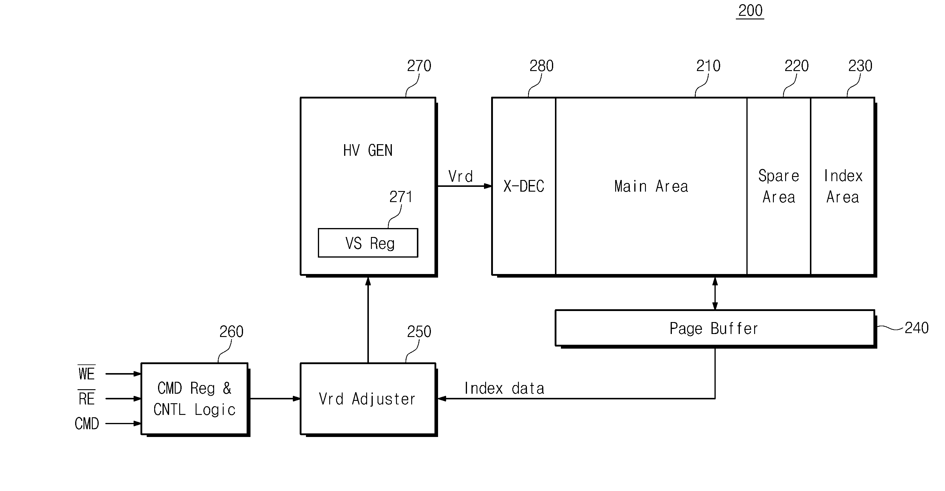
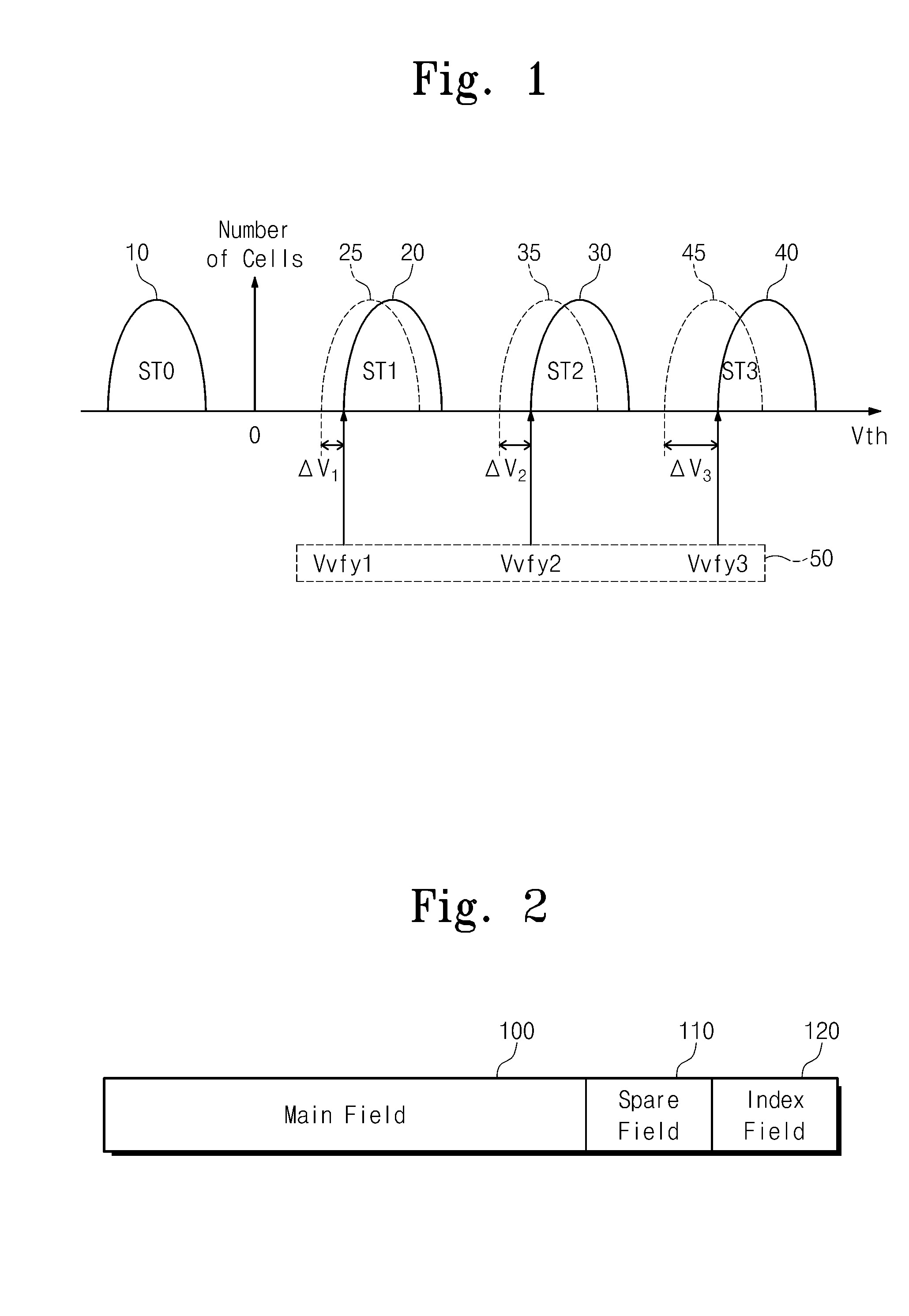
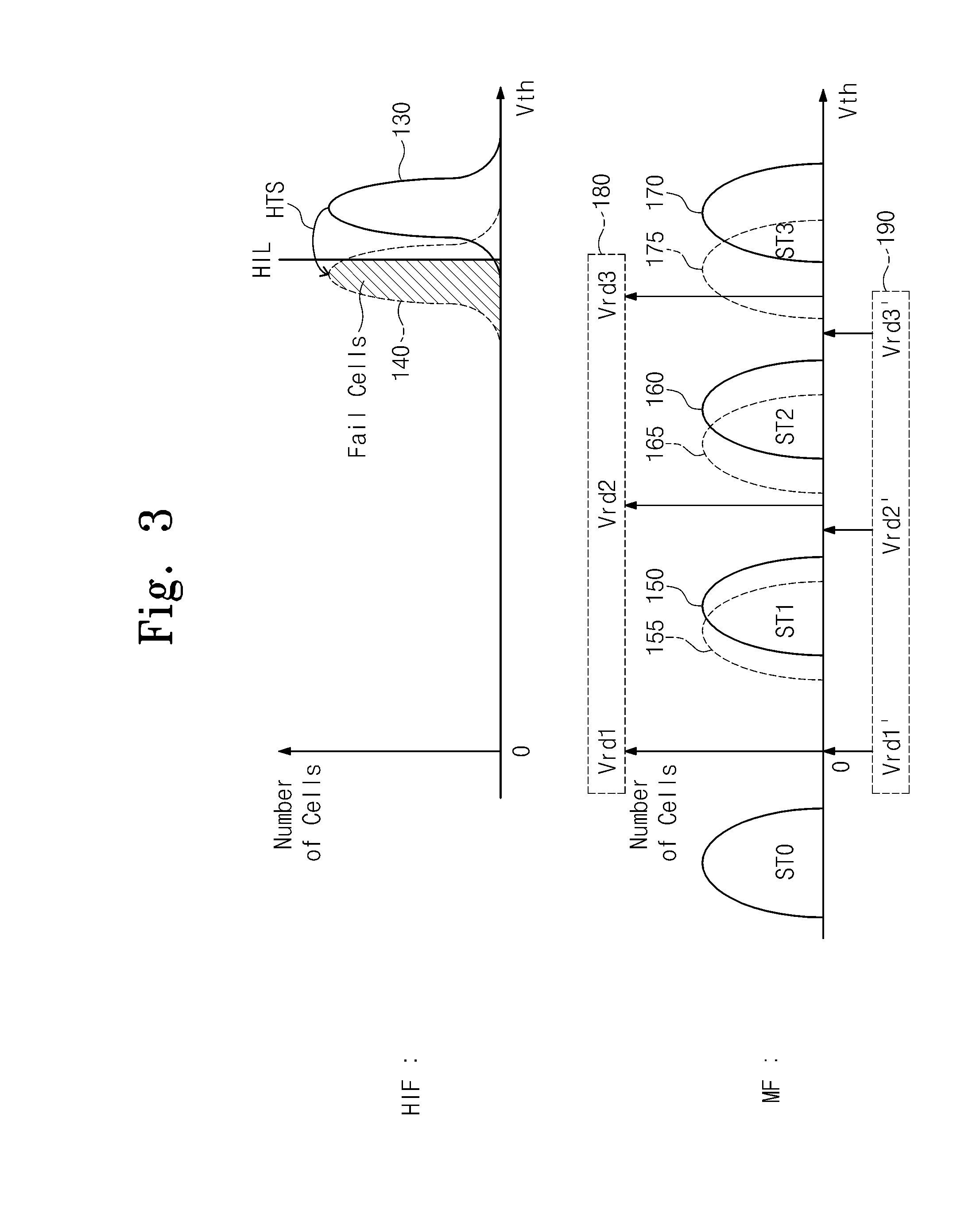
[0043]The present invention will now be described more fully with reference to the accompanying drawings, in which exemplary embodiments of the invention are shown. The invention, however, may be embodied in various different forms, and should not be construed as being limited only to the illustrated embodiments. Rather, these embodiments are provided as examples, to convey the concept of the invention to one skilled in the art. Accordingly, known processes, elements and techniques are not described with respect to some of the embodiments of the present invention. Throughout the drawings and written description, like reference numerals will be used to refer to like or similar elements.

[0044]Throughout this description, hot temperature stress (HTS) is provided as an example of a generic cause of losing charges injected into a floating gate of a flash memory cell. However, it is understood that HTS is just one of many potential causes for inducing charge loss. Further, a NAND flash me...


PUM


Abstract

A flash memory device includes a cell array and a read voltage adjuster. The cell array includes a first field having first memory cells and a second field having second memory cells. The read voltage adjuster determines a read voltage for reading first data from the first memory cells of the first field with reference to second data read from the memory cells of the second field.

Description

CROSS-REFERENCE TO RELATED APPLICATION[0001]A claim of priority is made to Korean Patent Application No. 10-2007-0064547, filed on Jun. 28, 2007, the subject matter of which is hereby incorporated by reference.BACKGROUND[0002]The present invention disclosed herein relates to semiconductor memory devices. More particularly, the present invention relates to a flash memory device capable of adjusting a read voltage.[0003]Semiconductor memory devices are generally classified as volatile or nonvolatile memories with respect to data storage. Volatile memories operate at a high frequency, but have a disadvantage with respect to data retention because they lose data without power. In contrast, nonvolatile memories are useful because they maintain data regardless of whether power is supplied. Nonvolatile semiconductor memories include, for example, read-only memories (ROMs), mask ROMs (MROMs), programmable ROMs (PROMs), erasable and programmable ROMs (EPROMs), and electrically erasable and p...

Claims


Application Information

Patent Timeline
IPC IPC(8): G11C16/04
CPCG11C11/5642G11C16/3454G11C16/26G11C16/30
Inventor KANG, DONG-KU
Owner SAMSUNG ELECTRONICS CO LTD
Why Eureka
Try Eureka