Methods for high temperature etching a high-k material gate structure
a gate structure and high-temperature etching technology, applied in the field of high-temperature etching of high-temperature materials, can solve the problems of affecting the quality of high-k materials
- Summary
- Abstract
- Description
- Claims
- Application Information
AI Technical Summary
Benefits of technology
Problems solved by technology
Method used
Image

Examples
Embodiment Construction
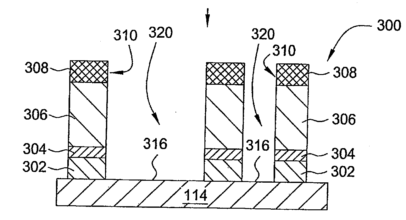
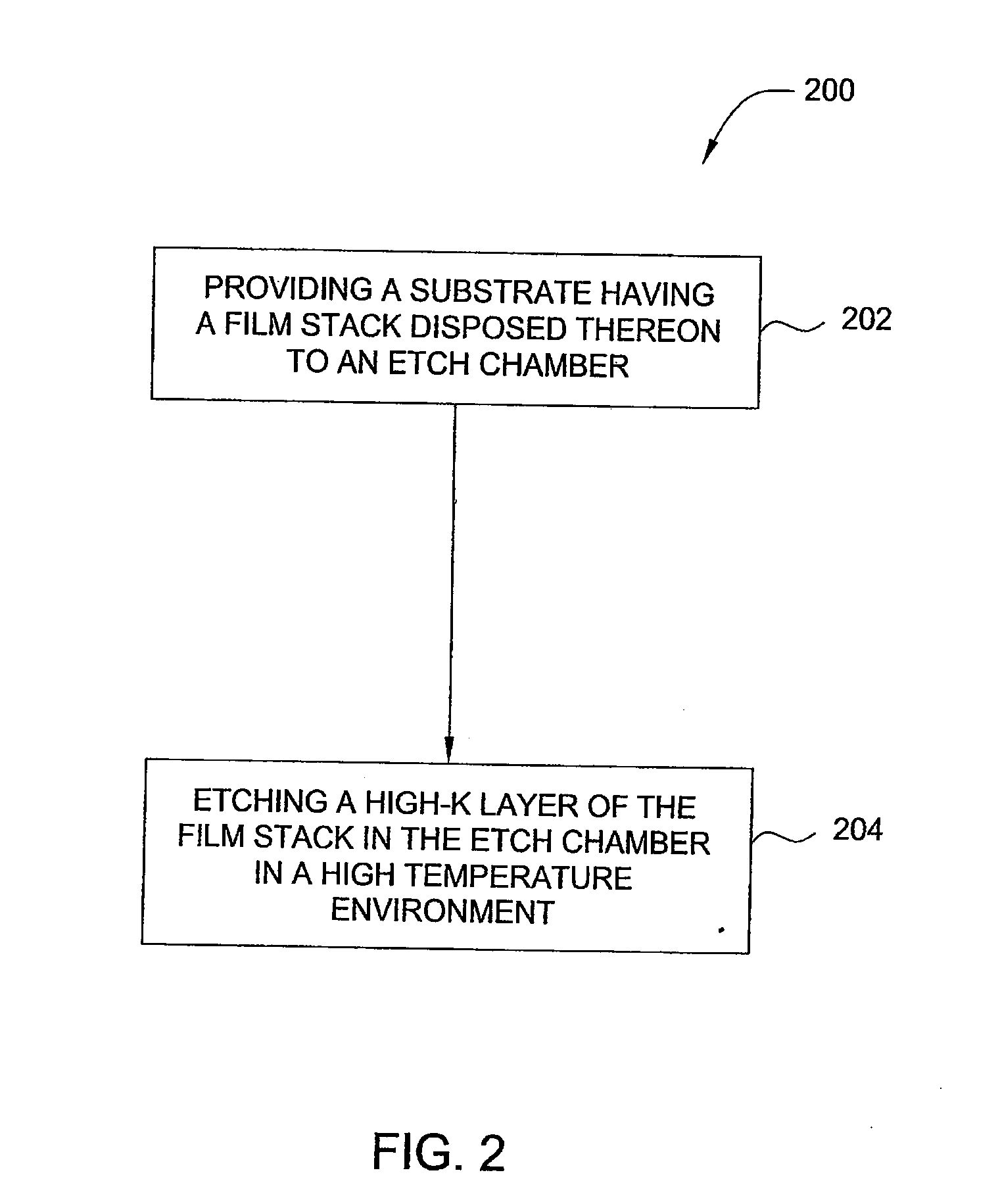
[0021]The invention generally relates to methods for etching a high-k material that is part of a film stack suitable for gate structure fabrication. In one embodiment, the high-k material of the gate structure film stack is etched at a temperature between about 100 degrees Celsius and about 250 degrees Celsius. In another embodiment, the high-k material along with an adjacent gate electrode layer are both etched at the similar temperature between about 100 degrees Celsius and about 250 degrees Celsius. The process described herein is advantageously suitable for high-k containing gate structure applications having submicron critical dimensions. The process also preserves a smooth, vertical, foot-free, zero silicon recess and straight profile of the formed gate structure. The etching process may be sequentially performed in a single etching chamber.
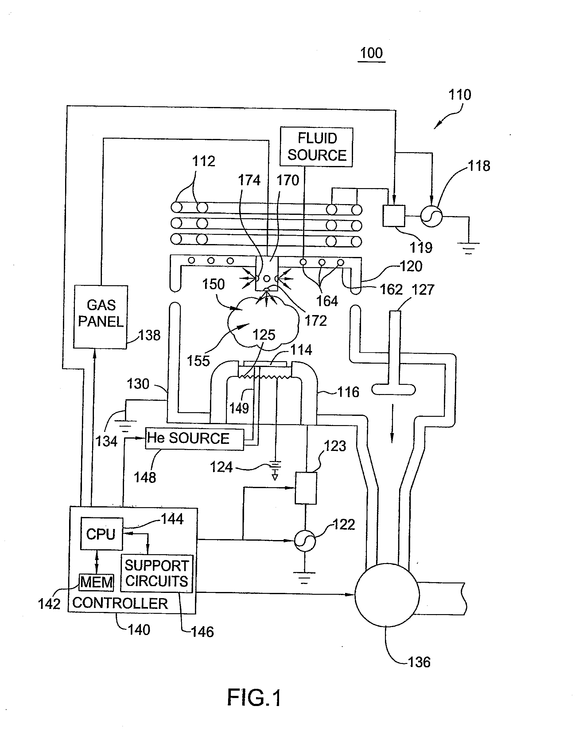
[0022]The etch process described herein may be performed in any suitable plasma etch chamber, for example, a Decoupled Plasma Source (DPS)...
PUM
| Property | Measurement | Unit |
|---|---|---|
| temperature | aaaaa | aaaaa |
| temperature | aaaaa | aaaaa |
| temperature | aaaaa | aaaaa |
Abstract
Description
Claims
Application Information
 - Generate Ideas
- Intellectual Property
- Life Sciences
- Materials
- Tech Scout
- Unparalleled Data Quality
- Higher Quality Content
- 60% Fewer Hallucinations
Browse by: Latest US Patents, China's latest patents, Technical Efficacy Thesaurus, Application Domain, Technology Topic, Popular Technical Reports.
© 2025 PatSnap. All rights reserved.Legal|Privacy policy|Modern Slavery Act Transparency Statement|Sitemap|About US| Contact US: help@patsnap.com