Integrated circuit and corresponding manufacturing method

a technology of integrated circuits and manufacturing methods, applied in the field of integrated circuits, can solve the problems of becoming more and more difficult to ensure the reliability and reproducibility of mass production, and a challenging task to form memory cells with minimal spatial extension

Inactive Publication Date: 2009-01-08
POLARIS INNOVATIONS LTD
View PDF6 Cites 3 Cited by
  • Summary
  • Abstract
  • Description
  • Claims
  • Application Information

AI Technical Summary

Problems solved by technology

With feature sizes that are becoming smaller and smaller and nowadays are well below 100 nm, it becomes a challenging task to form memory cells with minimum spatial extension, e.g. 4F2, where F is the critical dimension of the used patterning technology.
Also contact etching and etching mask openings for grooves for EUD (Extended U-Groove Device) transistors in the active area stripes between adjacent memory cell capacitors in a manner which is reliable and reproducible in mass production becomes more and more difficult.

Method used


Image

  • Integrated circuit and corresponding manufacturing method
  • Integrated circuit and corresponding manufacturing method
  • Integrated circuit and corresponding manufacturing method

Examples


Embodiment Construction

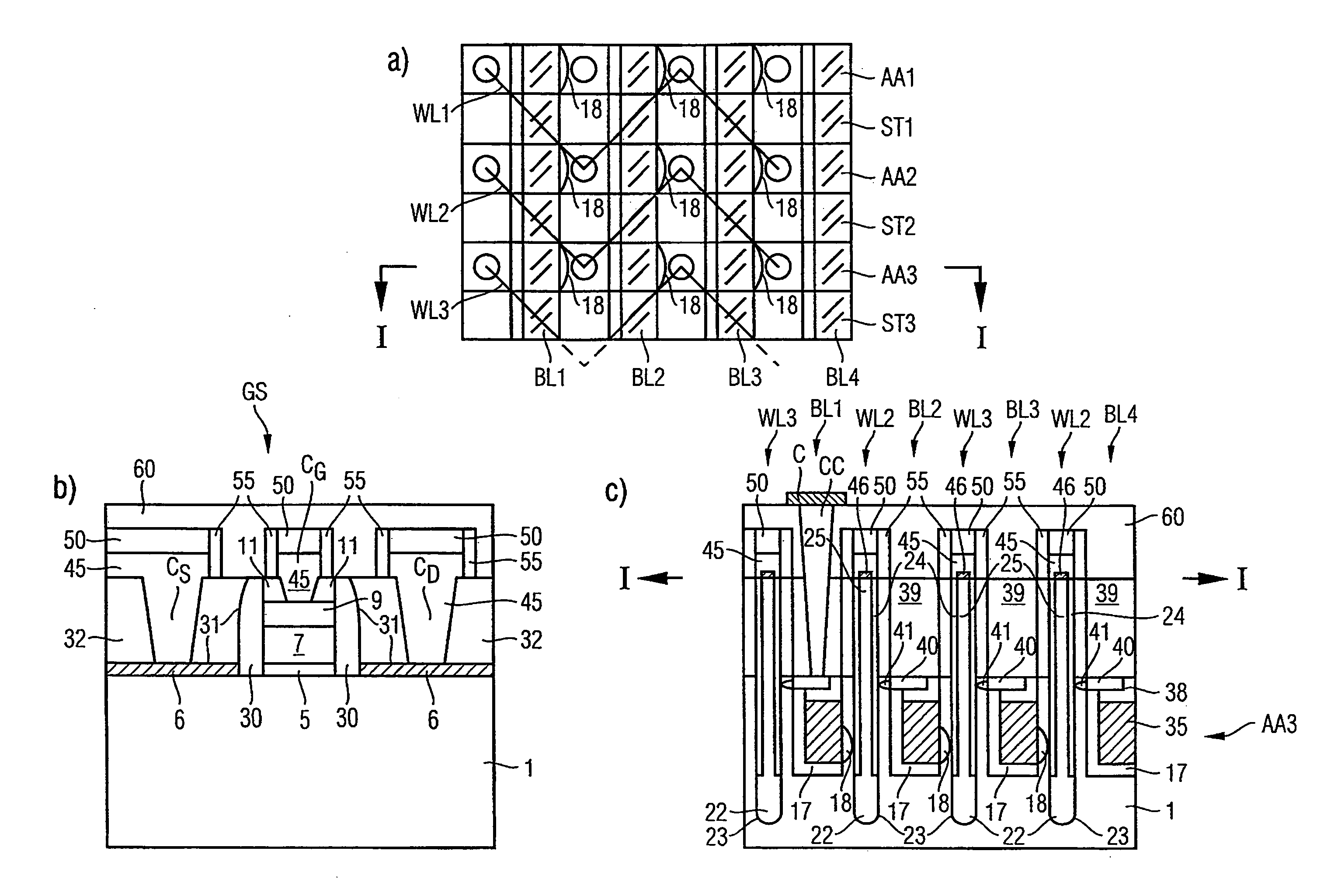
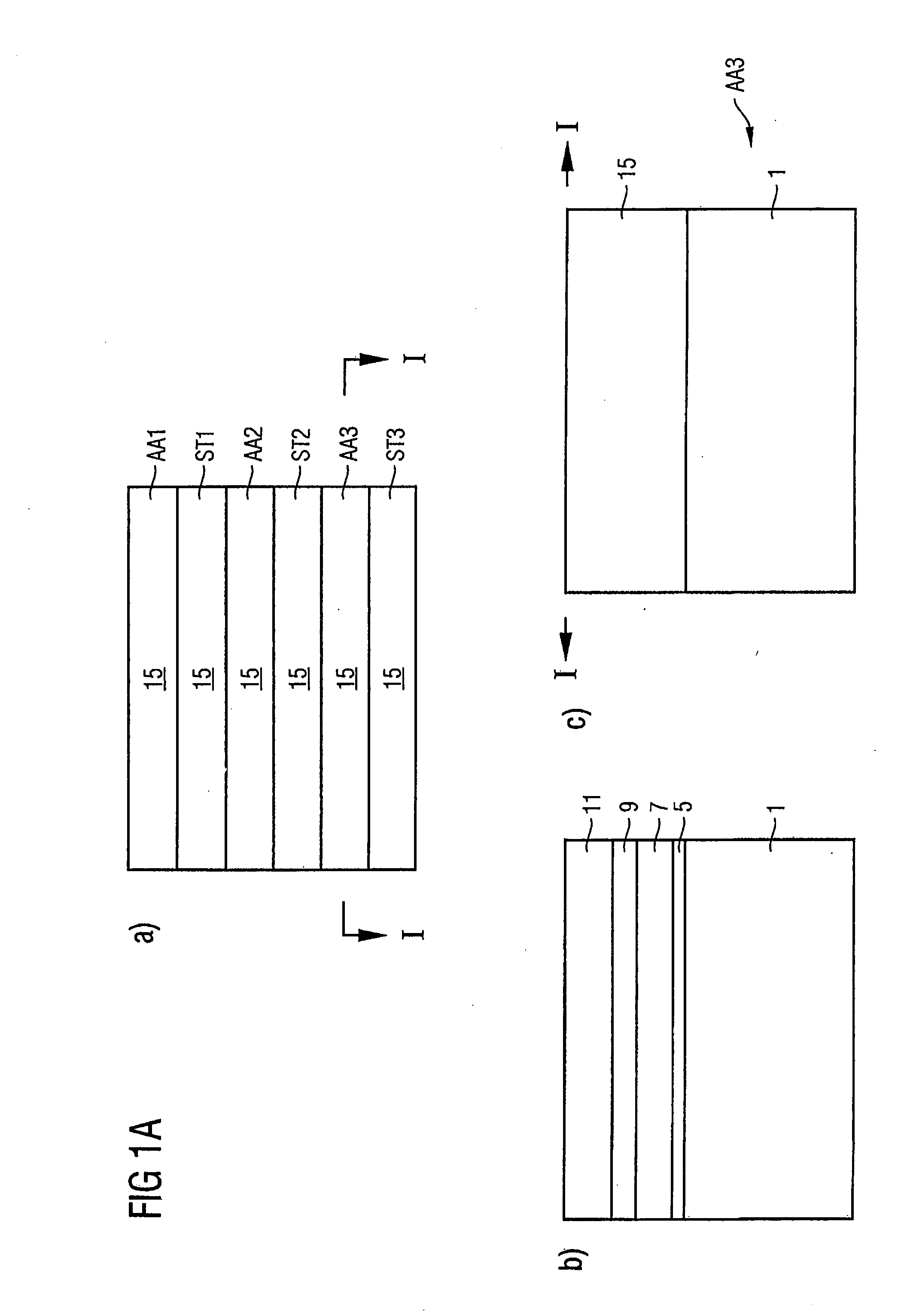
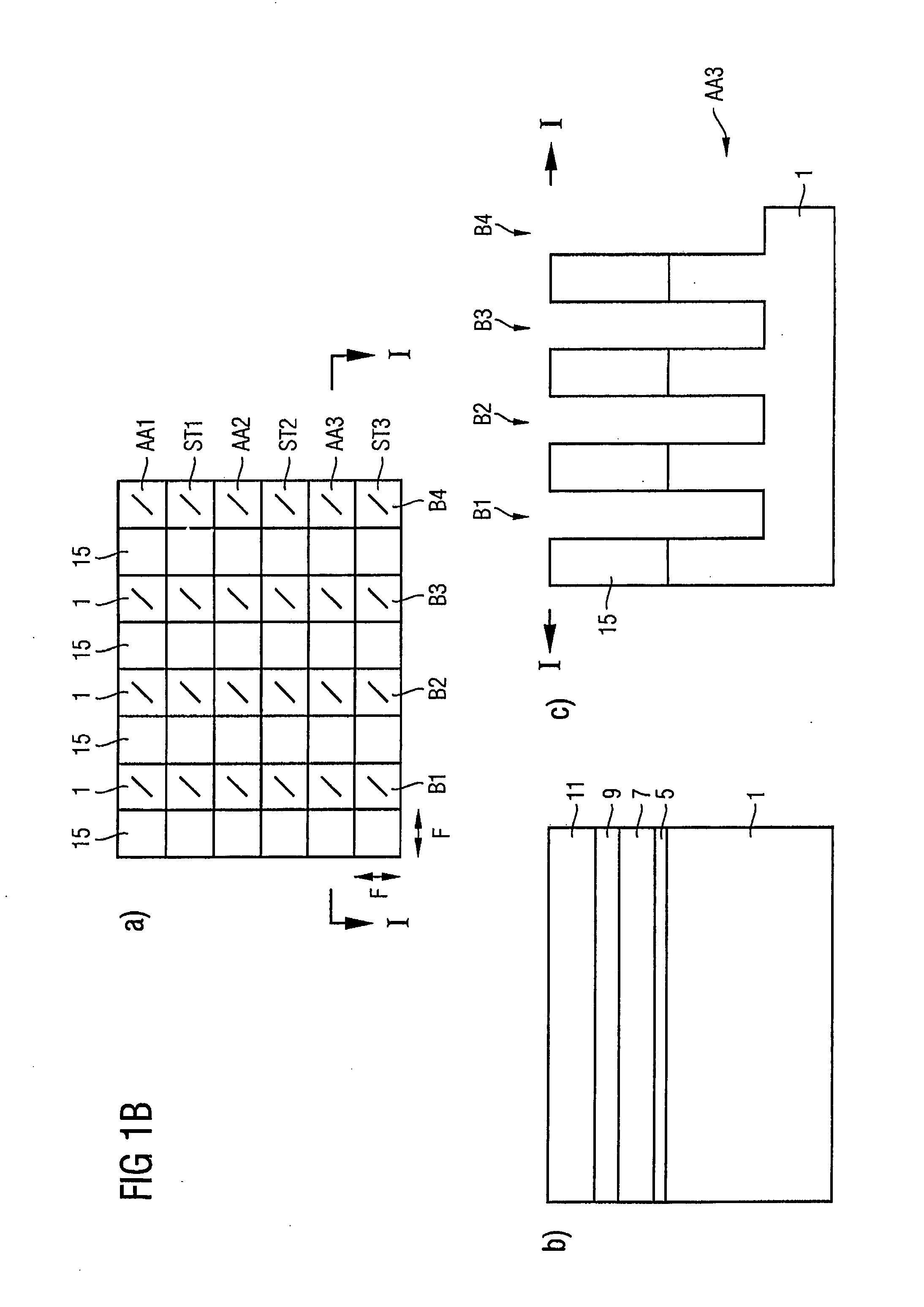
[0012]FIG. 1A-L show schematic layouts for illustrating a manufacturing method for a recessed channel transistor in an memory device according to an embodiment of the present invention, namely a) as plain view in a memory cell array area, b) a cross-section along a support device transistor processed in parallel in a peripheral support device area, and c) as cross-section along line I-I of a).

[0013]In FIG. 1A, reference sign 1 denotes a silicon semiconductor substrate. Formed in said silicon semiconductor substrate 1 are a plurality of parallel active area lines AA1, AA2, AA3, separated by a segmentation structure made of parallel shallow isolation trenches ST1, ST2, ST3 filled with a di-electric material, such as silicon oxide 15 (also called isolation segments). In this example, the silicon oxide layer 15 is also provided on top of said active area lines AA1, AA2, AA3, as may be obtained from FIG. 1A, c).

[0014]As becomes apparent from FIG. 1A, b), in the peripheral support device ...


PUM


Abstract

The present invention provides an integrated circuit including a field effect transistor formed in an active area segment of a semiconductor substrate, the transistor comprising:
    • a first and a second source/drain contact region; and
    • a channel region arranged in a groove formed in the active area segment and extending to a groove depth larger than a lower first contact depth,
wherein the second source/drain contact region is arranged at a vertical extension above the extension of the first source/drain contact region and a corresponding manufacturing method.

Description

BACKGROUND OF THE INVENTION[0001]1. Field of the Invention[0002]The present invention relates to an integrated circuit and a corresponding manufacturing method.[0003]2. Description of the Related Art[0004]Although in principle applicable to arbitrary integrated circuit devices, the following invention and the underlying problems will be explained with respect to integrated DRAM memory circuits in silicon technology, in particular, DRAM technology which is scaled down to below 100 nm generation and provides big challenges.[0005]DRAM memory circuits of today usually comprise stripe-like active areas, e.g. fabricated in silicon, separated by STI insulation trenches filled with a dielectric material such as silicon oxide.[0006]With feature sizes that are becoming smaller and smaller and nowadays are well below 100 nm, it becomes a challenging task to form memory cells with minimum spatial extension, e.g. 4F2, where F is the critical dimension of the used patterning technology. Also cont...

Claims


Application Information

Patent Timeline
Patent Type & Authority Applications(United States)
IPC IPC(8): H01L21/8242H01L27/108
CPCH01L27/10876H01L29/7827H01L29/66666H01L27/10894H10B12/053H10B12/09
Inventor MUEMMLER, KLAUSBAARS, PETERTEGEN, STEFAN
Owner POLARIS INNOVATIONS LTD
Why Eureka
Try Eureka