Display device, active matrix substrate, liquid crystald display device and television receiver

a liquid crystal display and active matrix technology, applied in static indicating devices, non-linear optics, instruments, etc., can solve the problems of image having a high spatial frequency blur, and achieve the effects of low luminance, high luminance, and high luminan

Inactive Publication Date: 2009-01-08
SHARP KK
View PDF25 Cites 49 Cited by
  • Summary
  • Abstract
  • Description
  • Claims
  • Application Information

AI Technical Summary

Benefits of technology

[0012]Thus, the display device of the present invention has pixels each of which has a pixel arrangement so that a low luminance area and a high luminance area surrounded by the low luminance area can be provided. This causes the high luminance area to deal with the total luminance or substantially the total luminance of an entire pixel (the light irradiation is carried out from the center part of a pixel) so that most of gradation displays are carried out. This allows an image having a high spatial frequency to be clearly displayed because of a great improvement in transfer characteristic in a high spatial frequency area.
[0033]As explained above, the display device of the present invention can clearly display an image having a high spatial frequency. Also, when this active matrix substrate is used for a display device, it is possible to form a high luminance area and a low luminance area which surrounds the high luminance area in each pixel corresponding to each pixel region so that an image having a high spatial frequency can be displayed clearly.

Problems solved by technology

However, when a display is carried out while maintaining a uniform luminance in each pixel, a problem arises that an image having a high spatial frequency blurs as illustrated in FIG. 21 (b).
Even though the conventional structure disclosed in patent document 1 includes the upper and lower sub-pixels having different luminance cannot sufficiently make an improvement in display blurring of an image having a high spatial frequency.

Method used


Image

  • Display device, active matrix substrate, liquid crystald display device and television receiver
  • Display device, active matrix substrate, liquid crystald display device and television receiver
  • Display device, active matrix substrate, liquid crystald display device and television receiver

Examples


Embodiment Construction

[0084]The following description deals with an embodiment of the present invention with reference to the FIG. 1 through FIG. 35.

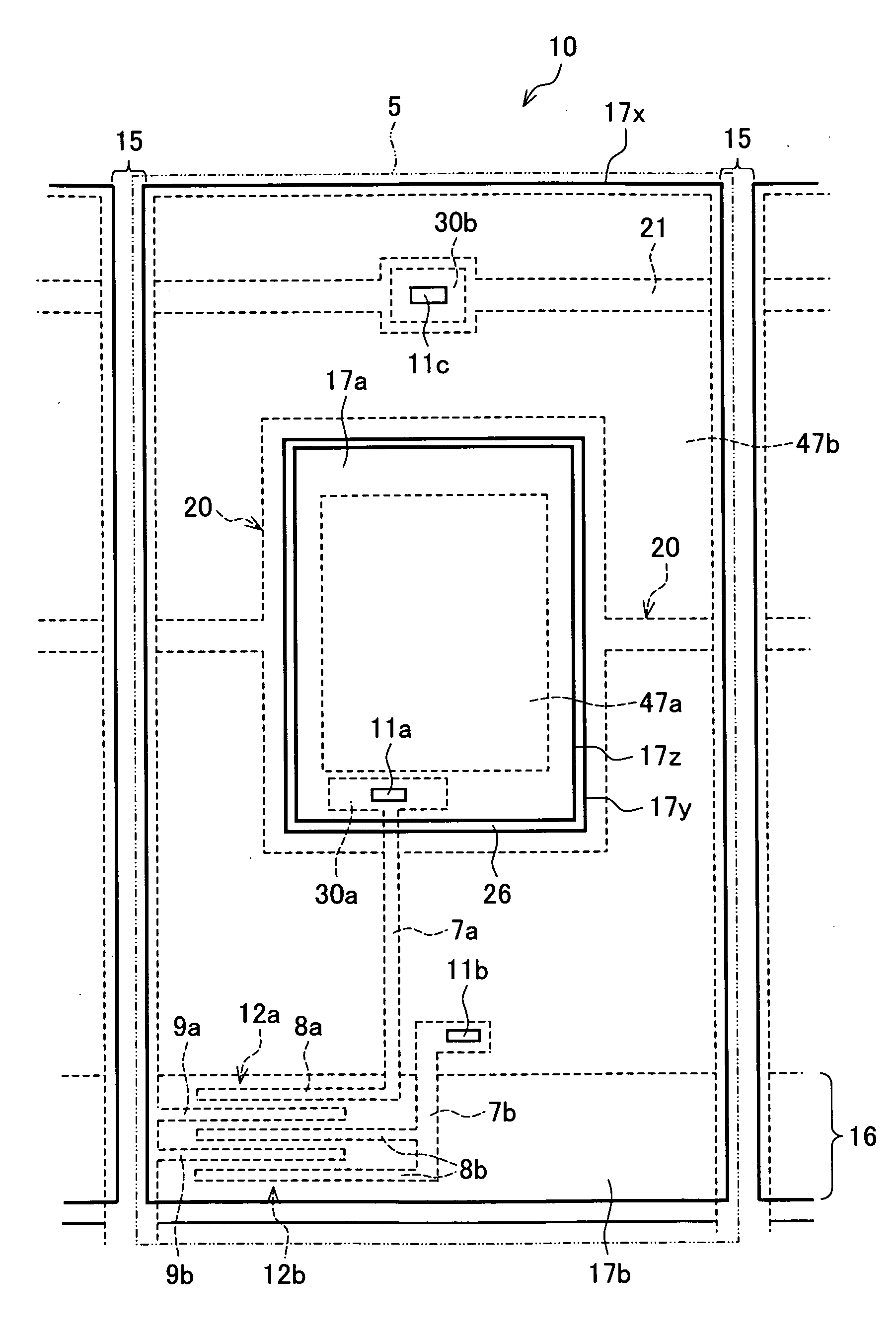
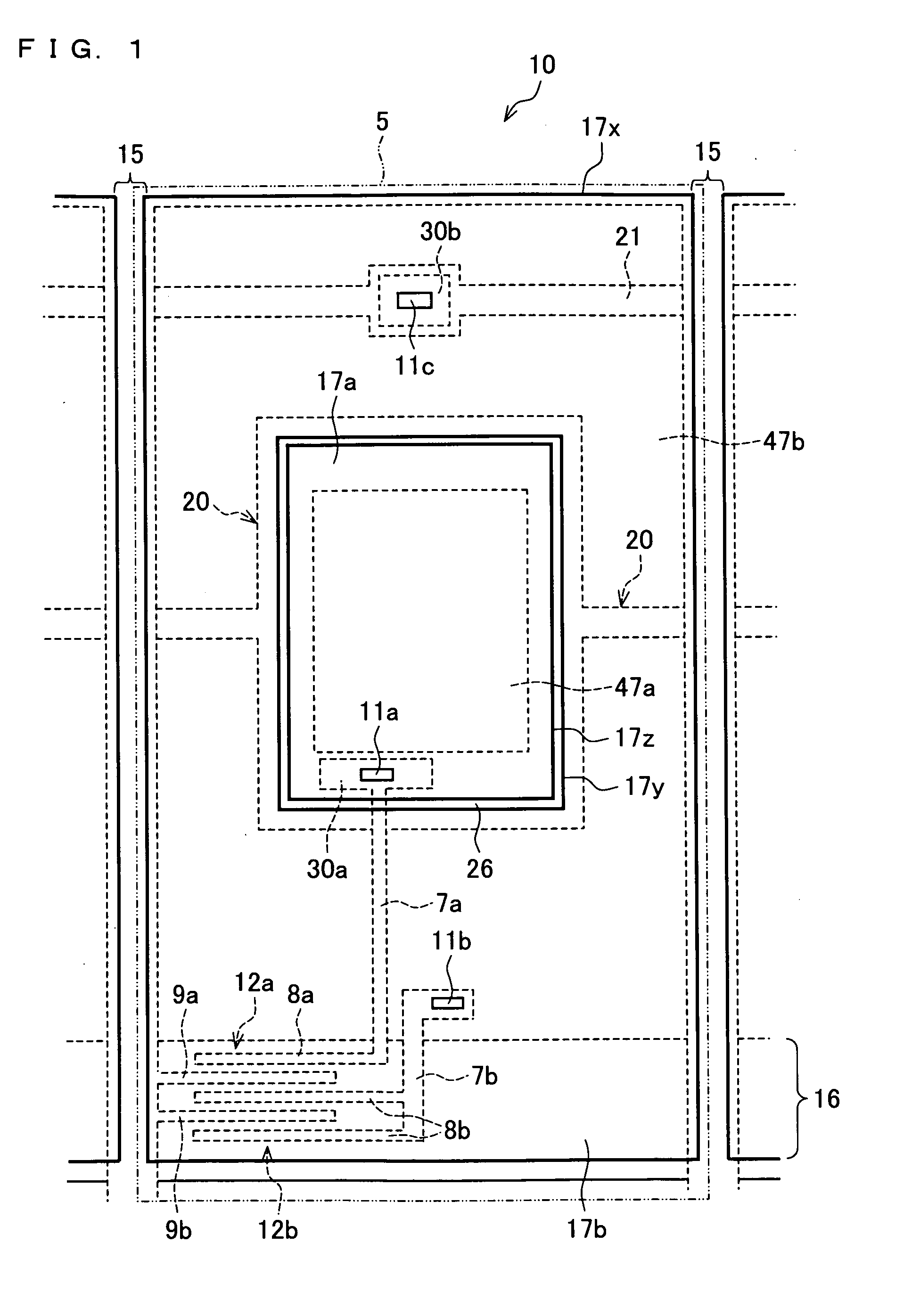
[0085]FIG. 1 is a perspective plain view illustrating a structure of an active matrix substrate in accordance with an embodiment of the present invention. As illustrated in FIG. 1, an active matrix substrate 10 includes a pixel region 5 arranged in matrix, a scan signal line 16 (along a row direction, in a transverse direction in FIG. 1) and a data signal line 15 (along a column direction, in an up-and-down direction in this figure) both lines provided so as to be intersected with each other, first retentive capacity wiring 20, and second retentive capacity wiring 21.

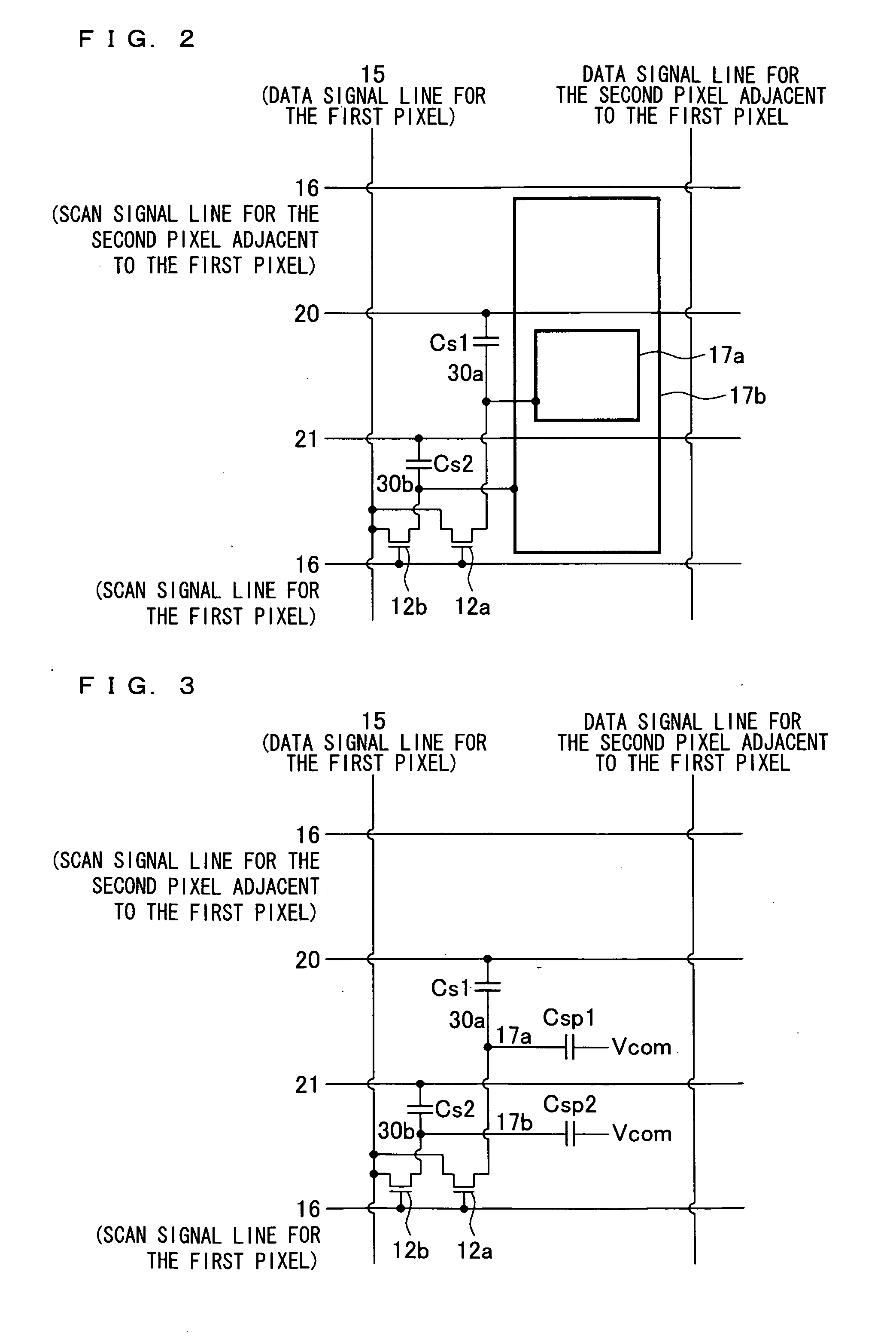
[0086]Each of the pixel regions 5 includes a first TFT (Thin Film Transistor) 12a, a second TFT 12b, a first sub-pixel electrode 17a, and a second sub-pixel electrode 17b.

[0087]The second sub-pixel electrode 17b has a rectangular shape which is hollowed out to have a hollow part. The second sub...


PUM


Abstract

In one embodiment of a display device, pixels are arranged in matrix, and a first luminance area (high luminance area) and a second luminance area (low luminance area) which surrounds the first luminance area and has a luminance lower than that of the first luminance area can be formed in each pixel. The display device which can clearly display an image having a high spatial frequency and an active matrix substrate to be used for the display device are provided.

Description

TECHNICAL FIELD[0001]The present invention relates to a display device such as a liquid crystal display device and to an active matrix substrate to be used for the display device.BACKGROUND ART[0002]FIG. 36 illustrates a structure of a conventional active matrix substrate used for a liquid crystal display device. As illustrated in FIG. 36, an active matrix substrate 700 includes a plurality of scan signal lines 716 and a plurality of data signal lines 715 both lines provided so as to be intersected with each other, TFTs (Thin Film Transistors) 712 each located in the vicinity of each intersection of a data signal line 715 and a scan signal line 716, and pixel electrodes 717. A scan signal line 716 also works as a gate electrode of a TFT 712. A source electrode 719 of the TFT 712 is connected to the data signal line 715. A drain electrode 708 is connected to a pixel electrode 717 through a drain lead-out electrode 707. Between the drain lead-out electrode 707 and the pixel electrode ...

Claims


Application Information

Patent Timeline
Patent Type & Authority Applications(United States)
IPC IPC(8): G09G3/36
CPCG02F1/13624G02F2001/134345G09G3/3648G09G2300/0426G09G2320/028G09G2300/0447G09G2300/0876G09G2310/0235G09G2300/0443G02F1/134345
Inventor UCHIDA, TOSHIHISATSUBATA, TOSHIHIDE
Owner SHARP KK
Why Eureka
Try Eureka