Semiconductor memory device

Inactive Publication Date: 2006-11-30
QIMONDA
View PDF7 Cites 33 Cited by
  • Summary
  • Abstract
  • Description
  • Claims
  • Application Information

AI Technical Summary

Benefits of technology

[0008] The present invention provides a semiconductor memory device with further reduc

Problems solved by technology

However, at present it is no more feasible to manufacture capacitors with further reduced lateral dimensions.
The shorter channel leads to higher leakage currents from drain to source.

Method used


Image

  • Semiconductor memory device
  • Semiconductor memory device
  • Semiconductor memory device

Examples


first embodiment

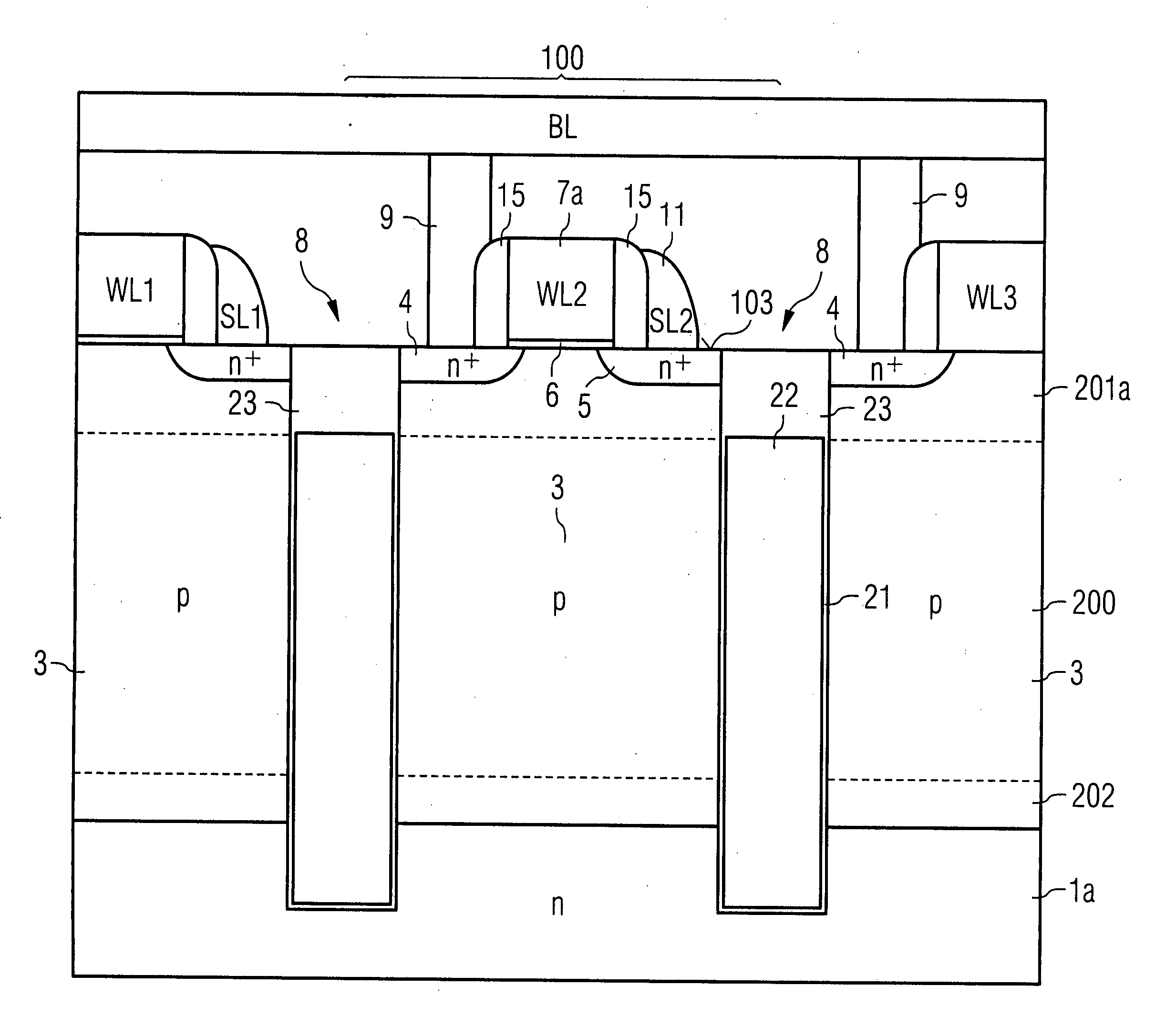
[0032]FIG. 3 illustrates a cross-section through a semiconductor memory device. At a first surface of a transistor body 3, a drain area 4 and a source area 5 are arranged. The transistor body 3 comprises a semiconductor material doped with a dopant of a first conductivity type, for example a p-type. The source and drain areas are doped with a dopant of a second different conductivity type, in the present example with an n-type dopant. On the first surface 103, a gate dielectric layer 6 is at least arranged between the source and the drain area and may extend in one embodiment over the drain area 4. A gate electrode 7a is arranged on top of the gate dielectric layer 6. The gate electrode 7a may be formed by a word line WL or is connected to the word line WL. Thus, a field effect transistor (FET) is provided formed by the source area 4, a gate structure comprising the gate dielectric layer 6 and the gate electrode 7a, and the source area 5.

[0033] The transistor body 3 is arranged on a...

second embodiment

[0046]FIG. 4 illustrates the semiconductor memory device. A recess 106 is formed in the first surface 103 between the drain 4 and the source area 5. The gate electrode 7b is formed in this trench. Thus the gate electrode 7b extends deep into the transistor body 3 forming a curved channel. A longer channel is provided guided along the outer surface of this recess.

[0047] A first advantage results in the fact that a longer channel reduces leakage currents from the drain area 4 to the source area 5 when the transistor is switched off. Thus the power consumption of the memory device is significantly reduced.

[0048] A further advantage results in the fact that charges which are stored far from the source and drain areas 4, 5 are still influencing the channel because it extends deep into the transistor body 3. Thus, the injected charges may be injected into areas distant to the source and drain areas. Similar to the first embodiment, a dopant concentration of a dopant is high in a first re...


PUM


Abstract

The semiconductor memory device comprises a plurality of memory cells. Each memory cell comprises a respective transistor and a respective capacitor unit. The transistor comprises a transistor body of a first conductivity type, a drain area and a source area each having a second conductivity type, the drain area and source area are embedded in the transistor body on a first surface of the transistor body, and a gate structure having a gate dielectric layer and a gate electrode, the gate structure is arranged between the drain area and the source area. An isolation trench is arranged adjacent to said transistor body, having a dielectric layer and a conductive material, wherein the isolation trench is at least partially filled with the conductive material. The conductive material is isolated by said dielectric layer from the transistor body. The capacitor unit is formed by the transistor body representing a first electrode and the conductive material representing the second electrode.

Description

TECHNICAL FIELD OF THE INVENTION [0001] The present invention relates to a semiconductor memory device. BACKGROUND OF THE INVENTION [0002] Although the invention can in principle be applied to any desired semiconductor memory device, the invention and its underlying problem will hereinafter be explained with reference to random access memory devices. [0003] A commonly known random access memory device comprises a plurality of memory cells each provided with one transistor and one capacitor, so-called one-transistor-one-capacitor-cells. A binary information is stored in the memory cell as a charge in the capacitor. A read out of the information is achieved by addressing the transistor via a bit line and a word line. A current flow of the charge from the capacitor through the transistor into the bit line is detected and interpreted via a reading decoder. For a reliable operation of the reading decoder a minimal charge is necessary thus demanding for a minimal capacitance of about 30 f...

Claims


Application Information

Patent Timeline
IPC IPC(8): H01L29/94
CPCH01L21/7624H01L27/10802H01L27/1087H01L29/945H01L29/66181H01L29/7841H01L27/10873H10B12/20H10B12/0387H10B12/05
Inventor ROSNER, WOLFGANGHOFMANN, FRANZSPECHT, MICHAELSTADELE, MARTIN
Owner QIMONDA
Why Eureka
Try Eureka