Gated semiconductor device and method of fabricating same

a semiconductor and gate technology, applied in the field of semiconductor devices, can solve the problems of affecting the performance of reverse tunneling, the disadvantages of method and structure, and the inability to meet the requirements of reverse tunneling, so as to reduce failure and increase manufacturing cost or time.

Inactive Publication Date: 2008-10-09
TAIWAN SEMICON MFG CO LTD
View PDF6 Cites 31 Cited by
  • Summary
  • Abstract
  • Description
  • Claims
  • Application Information

AI Technical Summary

Benefits of technology

[0017]These and other problems are generally solved or circumvented, and technical advantages are generally achieved, by preferred embodiments of the present invention that have been found to produce an optimum gate dielectric spacer height, widening the spacer etching process window without a significant increase in manufacturing cost or time, and to reduce failure due to reverse tunneling voltage (RTV).
[0018]In accordance with a preferred embodiment of the present invention, a method for fabricating a semiconductor device comprises forming an oxide layer on a semiconductor substrate, forming a first and a second poly (polycrystalline silicon) gate layer separated by an inter-gate dielectric, forming a hard mask including an oxide layer between two nitride layers, reducing a lateral dimension of the oxide layer relative to at least the upper nitride layer, forming a gate structure using the hard mask, and forming a dielectric layer over the gate structure. The dielectric layer preferably includes three layers in an ONO configuration, that is, having a nitride layer between two oxide layers, and after formation is etched back to expose the top of the hard mask in separate the spacer dielectric layer in two separate gate spacers. The method may further include laterally etching the first poly layer to create and undercut near the base of the gate structure. In a preferred embodiment, there are two such gate structures, and the undercut is formed on the exterior side of both of them. An oxide layer, subsequently formed over the gate structure, including the undercut exterior side of the first poly layer, conforms to the undercut side in a manner that creates a uniform region of oxide material adjacent the exterior side of the first poly layer.
[0020]In accordance with another preferred embodiment of the present invention, a semiconductor device comprises at least one gate structure, the gate structure including an oxide layer separating a first poly layer from a semiconductor substrate, and an inter-gate dielectric layer separating the first poly layer from a second poly layer. In this embodiment, a hard mask including an oxide layer between two nitride layers is disposed above the second poly layer. The middle oxide layer of the hard mask is reduced in lateral dimension relative to at least be nitride layer above it, so that a dielectric gate spacer formed on each side of the gate structure conforms to the preferably I-shaped hard mask, and self-aligns to the top of the reduced dimension oxide layer during formation. The dielectric gate spacers may be etched back to expose the top surface of the hard mask, and otherwise cover the sides of the respective gate structures except at their base, where one or both sides of the first poly layer portion of the gate structure are etched back laterally to create an undercut. The oxide layer, in this embodiment, is disposed over at least the undercut portion of the gate structure to create a uniform-thickness region. This uniform-thickness region, preferably present on the exterior side of each of the two gate structures, has been found to discourage RTV failure.

Problems solved by technology

Although adequate, this method and structure have disadvantages in certain applications.
In addition, with such small nodes, reverse tunneling performance problems may also become significant.

Method used


Image

  • Gated semiconductor device and method of fabricating same
  • Gated semiconductor device and method of fabricating same
  • Gated semiconductor device and method of fabricating same

Examples


Embodiment Construction

[0032]The making and using of the presently preferred embodiments are discussed in detail below. It should be appreciated, however, that the present invention provides many applicable inventive concepts that can be embodied in a wide variety of specific contexts. The specific embodiments discussed are merely illustrative of specific ways to make and use the invention, and do not limit the scope of the invention.

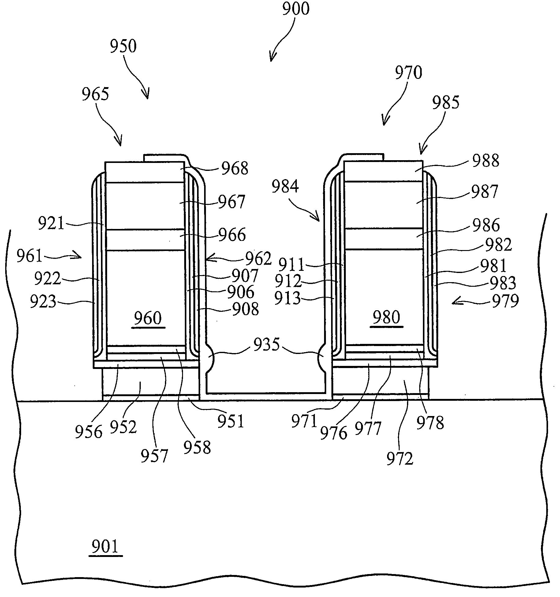
[0033]The present invention will be described with respect to preferred embodiments in a specific context, namely a dual-gate flash memory cell. The invention may also be applied, however, to other, similar semiconductor devices as well.

[0034]The present invention, then, is directed to a method for fabricating a semiconductor device, specifically a method for forming a flash memory cell or similar structure that in one embodiment provides an improved spacer-formation process window without adding significantly to manufacturing cost, and at the same time reduces the risk of re...


PUM

PropertyMeasurementUnit
diameteraaaaaaaaaa
dimensionsaaaaaaaaaa
thicknessaaaaaaaaaa

Abstract

A method for fabricating a gated semiconductor device, and the device resulting from performing the method. In a preferred embodiment, the method includes forming a hard mask for use in gate formation on one or more layers of alternately insulating and conducting material that have been formed on a substrate. The hard mask preferably includes three layers; a lower nitride layer, a middle oxide, and an upper nitride layer. In this embodiment, the middle oxide layer is formed with the rest of the hard mask, and then reduced in a lateral dimension, preferably using a DHF dip. A dielectric layer formed over the gate structure, including the hard mask, then etched back, self-aligns to be reduced-dimension oxide layer. In addition, where two conducting, that is gate layers are present, the lower layer is laterally reduced in dimension on at least one side to create an undercut.

Description

TECHNICAL FIELD[0001]The present invention relates generally to the field of semiconductor devices, and relates more particularly to flash memory cells and similar gated structures, which according to the present invention are fabricated in a fashion found to provide for a wider spacer-etching process window and to have other advantageous characteristics, especially when applied to semiconductor devices having relatively-small features.BACKGROUND[0002]Flash memory cells are a type of semiconductor device. Generally, semiconductor devices are very small components, or collections of components, formed on a piece of semiconductor material often referred to as the substrate. Flash memory cells, for example, feature a gate structure formed on the substrate, as will be explained in more detail below. In many current applications, the substrate is a round, thin slice of silicon or some similar material that has been cut from an ingot formed for this purpose. The substrate material is then...

Claims


Application Information

Patent Timeline
Patent Type & Authority Applications(United States)
IPC IPC(8): H01L29/788H01L21/336
CPCH01L21/28273H01L27/115H01L27/11521H01L29/42324H01L29/513H01L29/6656H01L29/7881Y10S438/945H01L29/40114H10B41/30
Inventor LIU, SHIH-CHANGSHEN, MING-HUILO, CHI-HSINTSAI, CHIA-SHIUNGCHU, YI-SHIN
Owner TAIWAN SEMICON MFG CO LTD
Why Eureka
Try Eureka