Piezoelectric switch for tunable electronic components

a technology of electronic components and piezoelectric switches, which is applied in the direction of relays, generators/motors, contacts, etc., can solve the problems of inability to achieve substantial reduction in the size of these switches, increase response time, and relatively low production costs, so as to reduce the lateral dimension, reduce the actuation voltage, and reduce the effect of lateral for

Inactive Publication Date: 2005-06-16
HRL LAB
View PDF57 Cites 33 Cited by
  • Summary
  • Abstract
  • Description
  • Claims
  • Application Information

AI Technical Summary

Benefits of technology

[0010] The present invention provides a novel layered (unimorph, bimorph or multimorph) piezoelectric switch that requires a very low actuation voltage (about 10 V), while keeping the overall lateral dimensions small (about 60 μm).
[0011] This is made possible by applying opposing (or crossed) actuation voltages across the length of the switch, causing a ‘S’ shaped switch deformation. The switch has a fast response time (about 2 microseconds) and avoids the problems associated with conventional electrostatic switches.
[0012] Additionally, this is made possible by a piezoelectric-electrostatic switch that uses a novel approach of combining the piezoelectric and electrostatic effects without using any extra electrodes on the active layer, allowing voltages significantly lower as compared to electrostatic switches of similar dimensions.
[0022] Compared to existing switch designs, the invention possesses substantially reduced lateral dimensions, while further lowering actuation voltages to about 10 V. This small size enables the invention to achieve much faster (about 1 microsecond) response times. In addition, a large restoring force can be generated to release the switch, thereby alleviating the severe problem of stiction associated with most switch designs.

Problems solved by technology

Also, as this type of switch is fabricated using existing integrated circuit (IC) processing technologies, production costs are relatively low.
This results in an increased response time.
A substantial reduction in the size of these switches is not possible as that significantly increases the actuation voltages.
Therefore, electrostatic actuation MEMS switches cannot be further miniaturized as required for further applications.
The large dimensions also reduce the restoring force for switch release, thus contributing to a ‘stiction’ problem that essentially renders the switch useless.
In particular, the contacting pads tend to adhere to each other after a prolonged use.

Method used


Image

  • Piezoelectric switch for tunable electronic components
  • Piezoelectric switch for tunable electronic components
  • Piezoelectric switch for tunable electronic components

Examples


first embodiment

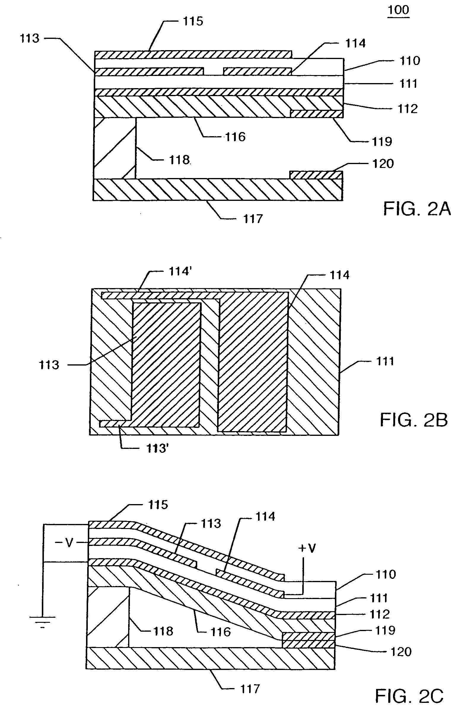
[0036]FIGS. 2A-2C show a switch according to the present invention. The switch, generally designated 100, is fabricated on a substrate 117 using generally known microfabrication techniques, such as masking, etching, deposition, and lift-off. In a preferred embodiment, the switch 100 is directly formed on the substrate 117. Alternatively, the switch 100 may be discreetly formed and then bonded to the substrate 117.

[0037] The switch 100 comprises an upper piezoelectric layer 110, a lower piezoelectric layer 111, a first electrode 112 placed under the lower layer 111, a second electrode 113 placed between the upper layer 110 and the lower layer 111, a third electrode 114 placed between the upper layer 110 and the lower layer 111, a fourth electrode 115 placed above the upper layer 110, and a Si3N4 layer 116 placed under the electrode 112. In the preferred embodiment, shown in the figure, the electrode 112 extends along the whole length of the piezoelectric layer 111, in order to avoid ...

third embodiment

[0067]FIGS. 7A-7B show a switch according to the present invention, where only three electrodes are used, and cross voltages are applied to the upper and lower electrodes.

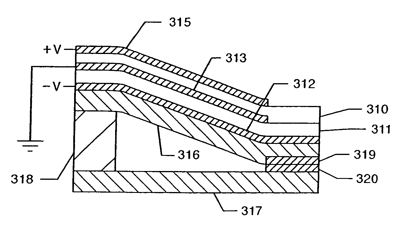
[0068]FIG. 7A shows a switch 300 comprising an upper piezoelectric layer 310, a lower piezoelectric layer 311, a first or lower electrode 312 placed under the lower layer 311, a second or middle electrode 313 placed between the upper layer 310 and the lower layer 311, and a third or upper electrode 315 placed above the upper layer 310. A Si3N4 layer 316 is connected to the electrode 312 and placed under the electrode 312. The switch 300 is placed above a substrate 317 and spaced from the substrate 317 by means of a spacer 318. Additionally, a first contact pad 319 is provided under the second electrode 312 and a second contact pad 320 is provided above the substrate 317.

[0069] Also in the third embodiment, an ‘S’ shaped deformation or deflection is obtained upon application of a voltage, as shown in FIG. 7B. The ‘...

fourth embodiment

[0071]FIGS. 8A-8C show a switch according to the present invention, where switching occurs according to a combination between electrostatic effect and piezoelectric effect. In particular, combination of the electrostatic effect with the embodiment of FIGS. 7A and 7B is shown.

[0072]FIG. 8A shows a switch 400 comprising an upper piezoelectric layer 410, a lower piezoelectric layer 411, a first or lower electrode 412 placed under the lower layer 411, a second or middle electrode 413 placed between the upper layer 410 and the lower layer 411, and a third or upper electrode 415 placed above the upper layer 410. A Si3N4 layer 416 is connected to the electrode 412 and placed under the electrode 412. The switch 400 is placed above a substrate 417 and spaced from the substrate 417 by means of a spacer 418. Additionally, a first contact pad 419 is provided under the second electrode 412 and a second contact pad 420 is provided above the substrate 417. The distance between contact pads 419 and...


PUM

PropertyMeasurementUnit
actuation voltagesaaaaaaaaaa
actuation voltageaaaaaaaaaa
response timeaaaaaaaaaa

Abstract

A piezoelectric switch for tunable electronic components comprises piezoelectric layers, metal electrodes alternated with the layers and contact pads. Cross voltages are applied to the electrodes, in order to obtain an S-shaped deformation of the switch and allow contact between the contact pads. Additionally, a further electrode can be provided on a substrate where the switch is fabricated, to allow an additional electrostatic effect during movement of the piezoelectric layers to obtain contact between the contact pads. The overall dimensions of the switch are very small and the required actuation voltage is very low, when compared to existing switches.

Description

CLAIM OF BENEFIT OF PROVISIONAL APPLICATION [0001] This application claims the benefit of U.S. provisional application Ser. No. 60 / 420,175 filed on Oct. 21, 2002, which is incorporated herein by reference in its entirety. CROSS-REFERENCE TO RELATED APPLICATIONS [0002] The present document is related to the copending and commonly assigned patent application documents entitled “Variable Capacitance Membrane Actuator for Wide Band Tuning Microstrip Resonators and Filters,” Ser. No. ______ (Attorney Docket No. 620760), and “Piezoelectric Actuator for Tunable Electronic Components,” Ser. No. ______ (Attorney Docket No. 620724), which are all filed of even date herewith. The contents of these related applications are hereby incorporated by reference herein.FIELD OF THE INVENTION [0003] The present invention relates to micro-electromechanical systems (MEMS) and, in particular, to a micromachined piezoelectric switch for tunable electronic components which can achieve substantial deflection...

Claims


Application Information

Patent Timeline
Patent Type & Authority Applications(United States)
IPC IPC(8): H01H1/00H01H57/00H01H59/00H01L41/09H01L41/24H02N2/04
CPCH01H1/0036H01H57/00H01H59/0009H01H2057/006H01L41/094H01L41/1876Y10T29/49105H01L41/332H01G5/18H01G5/40Y10T29/49107Y10T29/42H01L41/318H10N30/2042H10N30/8554H10N30/078H10N30/082
Inventor MEHTA, SARABJIT
Owner HRL LAB
Why Eureka
Try Eureka