
Non-volatile memory device

Active Publication Date: 2009-01-08
KIOXIA CORP
View PDF4 Cites 23 Cited by
  • Summary
  • Abstract
  • Description
  • Claims
  • Application Information

AI Technical Summary

Benefits of technology

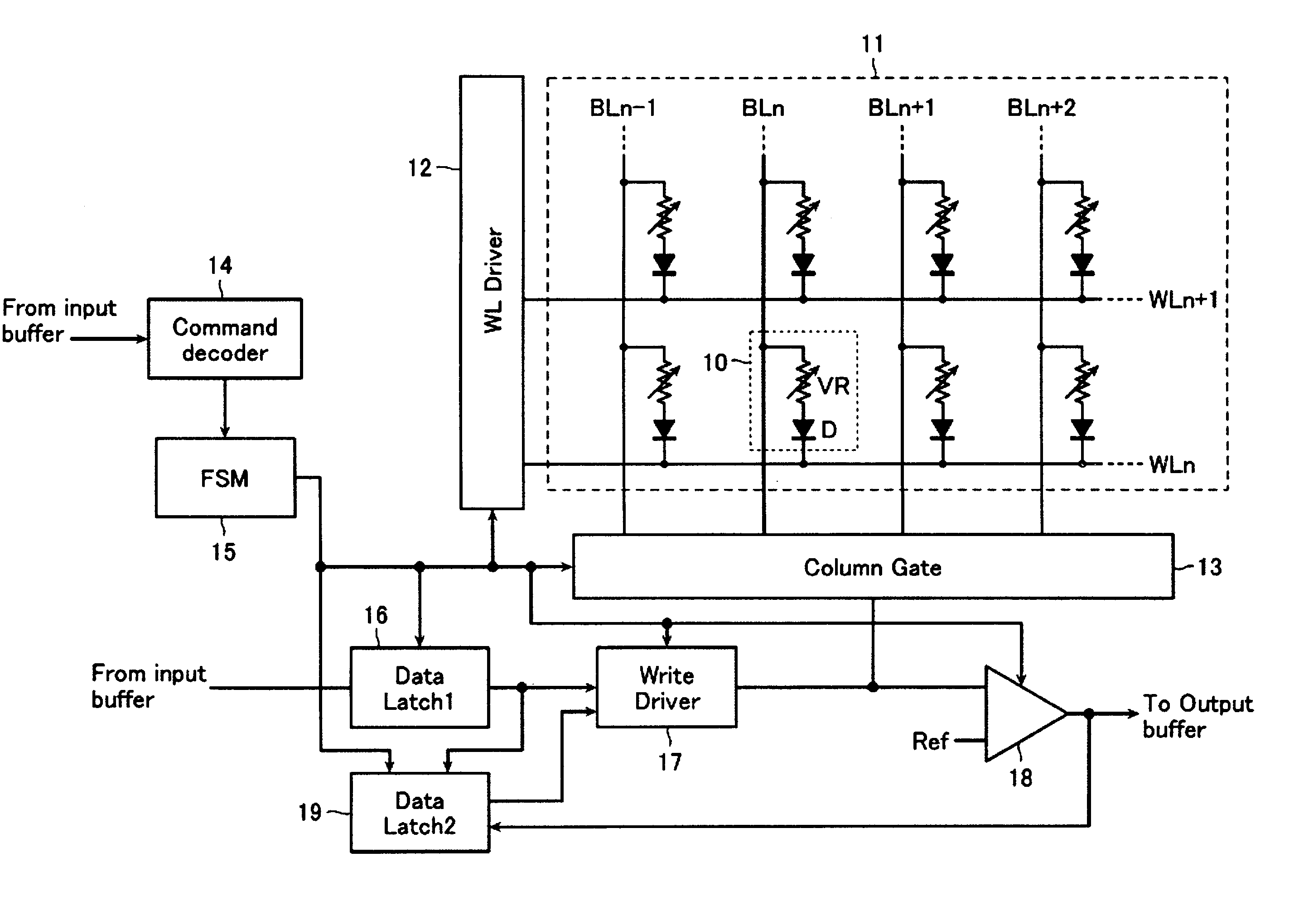
[0010]According to an aspect of the present invention, there is provided a nonvolatile memory device including: a memory cell array including memory cells each having a variable resistance element for nonvolatilely storing data identified by an electrically rewritable resistance value; a first data latch storing write and erase data to be written on a given group of memory cells of the memory cell array for a write and erase operation; and a second data latch storing reference data for performing a compensation operation of the given group to compensate write and erase disturbance accompanied by the write or erase operation.
[0011]According to another aspect of the present invention, ther

Problems solved by technology

When the cross-point-type cell array is configured without using a rectifying element, write disturbance occurs for unselected cells due to crosstalk generated in a write operation.
In the ReRAM, when gaps between the bit lines or the word lines decreases for implementing high-density and high integration, write disturbance (or erase disturbance) for unselected memory cells occurs due to capacitive coupling in a write (or erase) operation.

Method used


Image

  • Non-volatile memory device
  • Non-volatile memory device
  • Non-volatile memory device

Examples


Embodiment Construction

[0033]Hereinafter, embodiments of the present invention will be described with reference to the accompanying drawings.

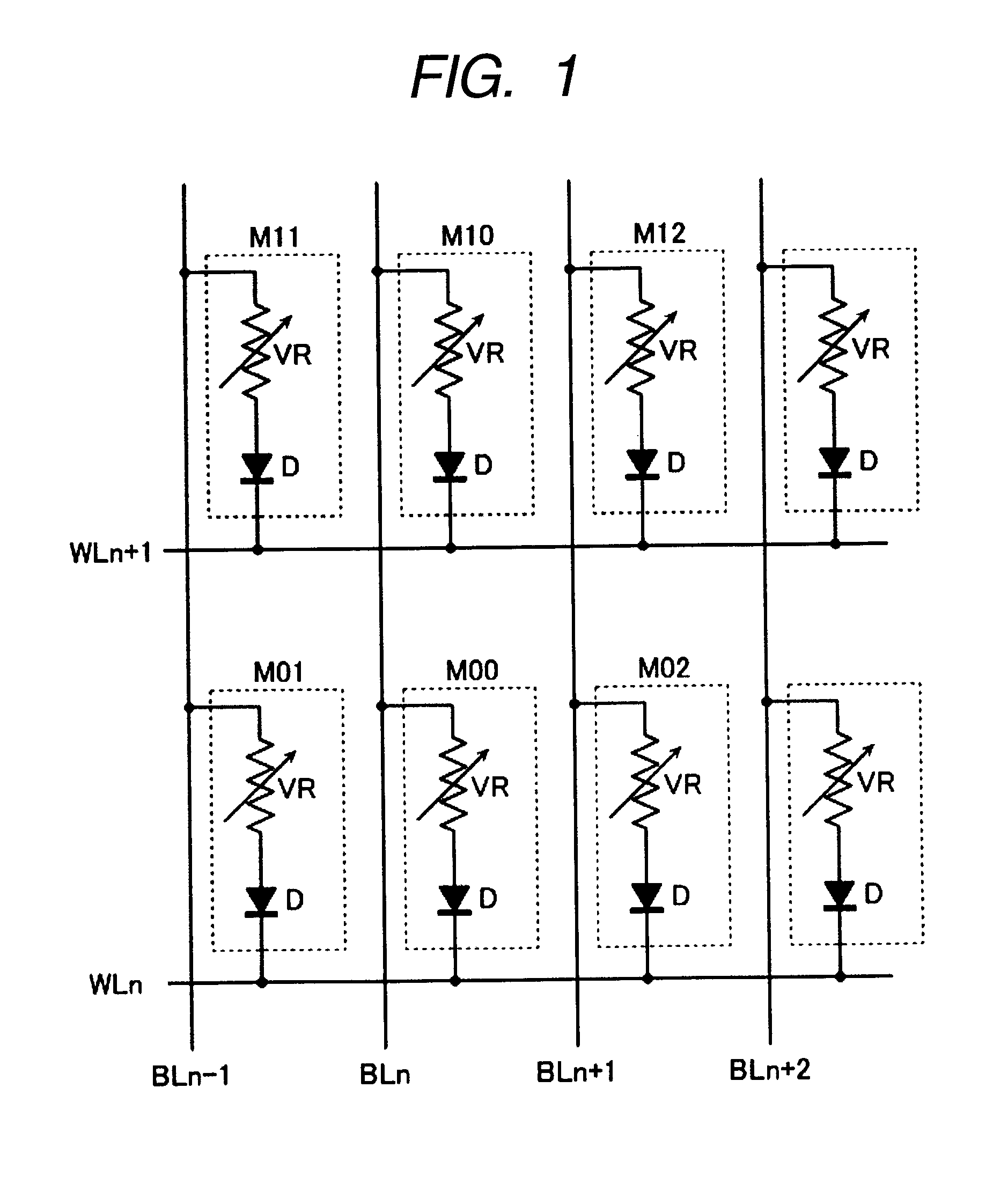
[0034]FIG. 1 shows the configuration of a memory cell array of a non-volatile memory according to an embodiment of the present invention. In the memory cell array, wirings (herein after, referred to as word lines) WL extending in the row direction (direction X) and wirings (herein after, referred to as bit lines) BL extending in the column direction (direction Y) which intersecting each other are disposed, and a memory cell in which a variable resistance element VR and a rectifying device D are stacked is disposed at each intersection thereof. In other words, the variable resistor element VR has one end connected to a bit line BL and the other end connected to a word line WL through the rectifying device D.

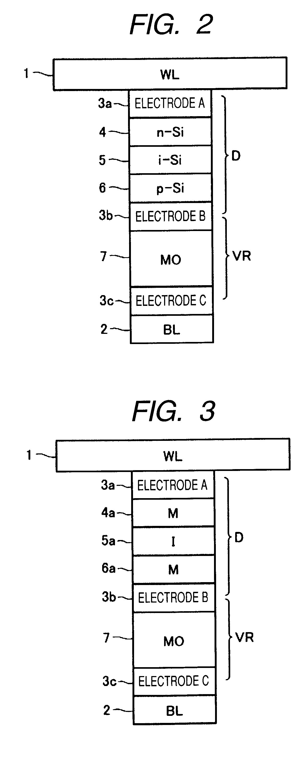
[0035]FIGS. 2 and 3 show the stacked structure of the variable resistance element VR and the rectifying device D that constitute the memory cell between the word l...


PUM


Abstract

According to one embodiment, a nonvolatile memory device includes: a memory cell array including memory cells each having a variable resistance element for nonvolatilely storing data identified by an electrically rewritable resistance value; a first data latch storing write and erase data to be written on a given group of memory cells of the memory cell array for a write and erase operation; and a second data latch storing reference data for performing a compensation operation of the given group to compensate write and erase disturbance accompanied by the write or erase operation.

Description

CROSS-REFERENCE TO RELATED APPLICATIONS[0001]This application is based upon and claims the benefit of priority from Japanese Patent Application No. 2007-147817, filed Jun. 4, 2007, the entire contents of which are incorporated herein by reference.BACKGROUND OF THE INVENTION[0002]The present invention relates to a non-volatile memory device that stores resistance value information of a variable resistance element, which can be electrically rewritable, in a non-volatile manner.[0003]Recently, as non-volatile memory devices, ReRAMs (Resistive Random Access Memory) that store resistance value information of an electrically-rewritable variable resistance element in a non-volatile manner have been attracted attention, and researches for the memory devices have been actively performed.[0004]The variable resistance element as a memory element of the ReRAM is configured by an electrode / a metal oxide / an electrode. It is known that there are two types of operation principles in the variable re...

Claims


Application Information

Patent Timeline
IPC IPC(8): G11C11/00G11C7/00
CPCG11C13/0007G11C13/0069G11C2213/72G11C2013/0092G11C2213/32G11C13/0097
Inventor TOKIWA, NAOYAKANDA, KAZUSHIGEEDAHIRO, TOSHIAKIHOSONO, KOJIFUTATSUYAMA, TAKUYAOHSIMA, SHIGEO
Owner KIOXIA CORP
Learn More