Integrated circuit device

a technology of integrated circuits and circuits, applied in the direction of inductances, basic electric elements, continuous variable inductances/transformers, etc., can solve the problems of little technological advancement in the spacing of i/o (input/output) pads of the chip, and the obstacle to higher integration of integrated circuit devices

Active Publication Date: 2009-01-15
RENESAS ELECTRONICS CORP
View PDF7 Cites 6 Cited by
  • Summary
  • Abstract
  • Description
  • Claims
  • Application Information

AI Technical Summary

Benefits of technology

[0020]In accordance with the present invention, it is possible to freely change coil position, mutual inductance and resonance frequency after chip packaging. This makes it possible to realize high-quality signal transmission.

Problems solved by technology

However, there has been little technological advance with regard to the spacing of I / O (input / output) pads of the chip.
As a consequence, the area occupied by the I / O portions is large and this has become a major obstacle to higher integration of integrated circuit devices.

Method used


Image

  • Integrated circuit device
  • Integrated circuit device
  • Integrated circuit device

Examples


Embodiment Construction

[0053]Next, an embodiment of the present invention will be described based upon the drawings.

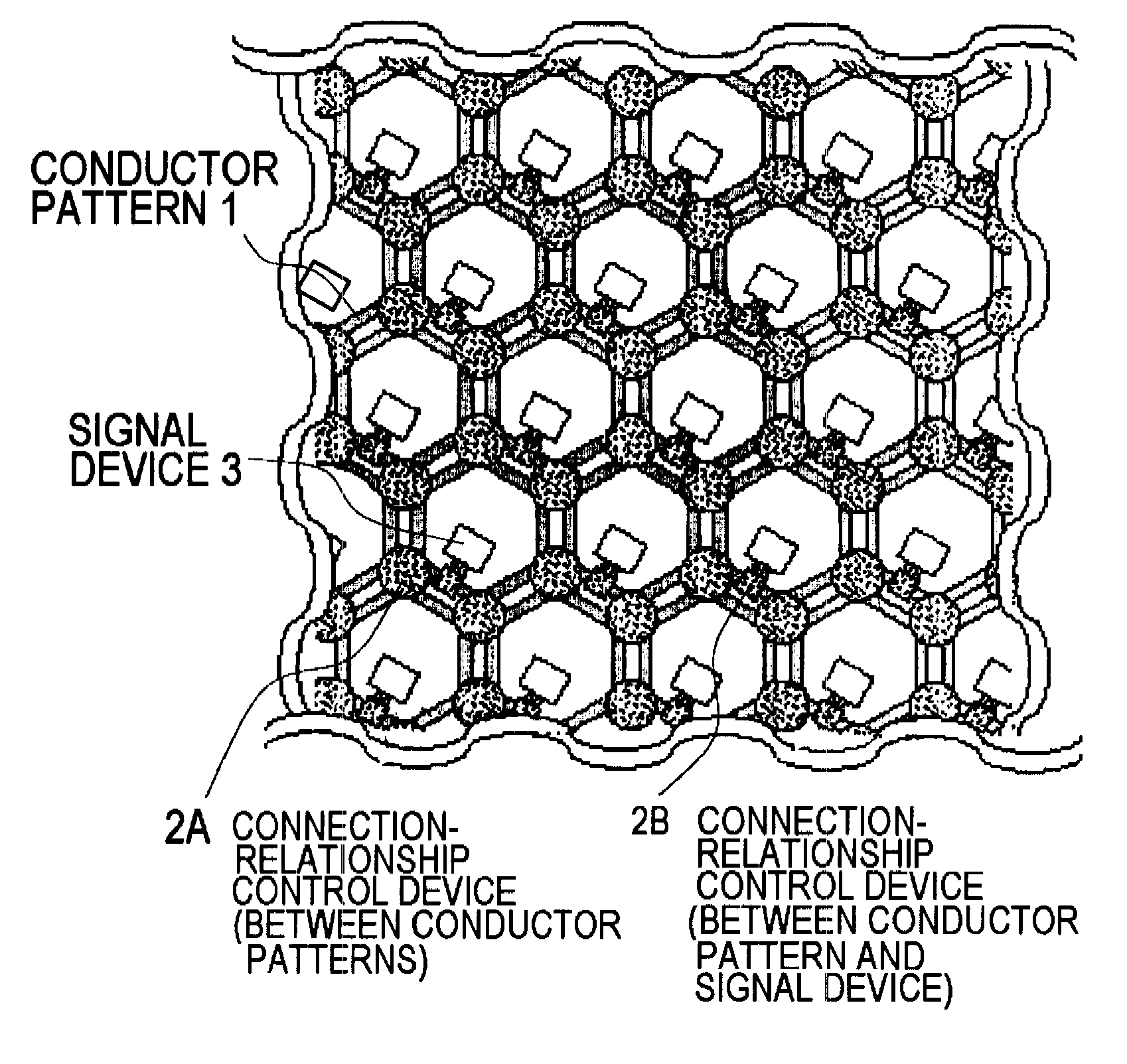
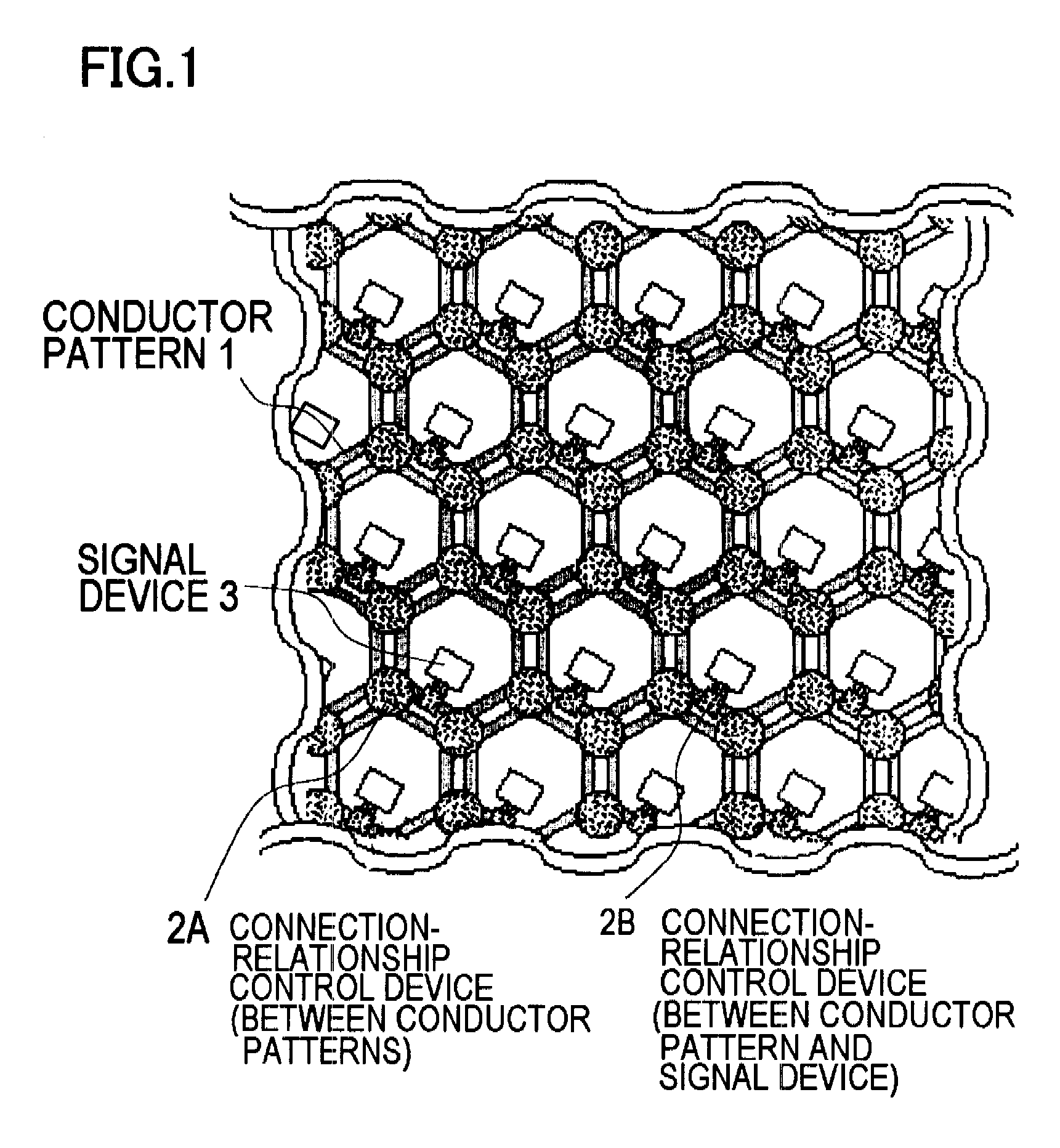
[0054]FIG. 1 is schematic planar view of a chip constituting an integrated circuit device according to an embodiment of the present invention. As illustrated in FIG. 1, a plurality of conductor patterns 1 for forming a coil, connection-relationship control devices 2A and 2B and a signal device 3 basically are formed on a surface layer or inner layer of a chip, which serves as a semiconductor substrate. The signal device 3 receives a current signal generated in a coil, or supplies a current signal to the coil, or does both. The integrated circuit device according to the present invention is obtained by stacking such chips in the vertical direction and performs signal transmission by electromagnetic coupling between opposing coils of the chips.

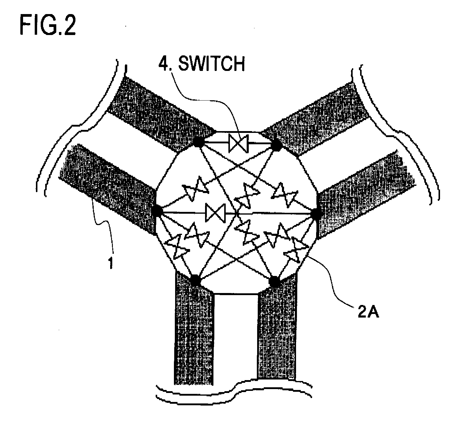
[0055]The first connection-relationship control device 2A is placed between ends of adjacent conductor patterns 1 and, after the chips are stacked, is c...


PUM


Abstract

Provided on a chip are a plurality of conductor patterns for forming a coil, and a connection-relationship control device for controlling connection between adjacent conductor patterns. By switching the connection relationship of the conductor patterns by the connection-relationship control device, it is possible to form a coil of a desired shape at a desired position.

Description

[0001]This invention relates to an integrated circuit device in which signal transmission is performed utilizing electromagnetic coupling by electromagnetic induction coils between chips stacked in the vertical direction.BACKGROUND ART[0002]Progress in microfabrication techniques applied in recent semiconductor manufacturing processes has been accompanied by higher integration of circuits incorporated in integrated circuit devices. However, there has been little technological advance with regard to the spacing of I / O (input / output) pads of the chip. As a consequence, the area occupied by the I / O portions is large and this has become a major obstacle to higher integration of integrated circuit devices.[0003]Accordingly, in recent years an integrated circuit device has been developed in which chips on which electromagnetic induction coils have been formed are stacked vertically and signal transmission is performed using opposing electromagnetic induction coils between chips (see Paten...

Claims


Application Information

Patent Timeline
Patent Type & Authority Applications(United States)
IPC IPC(8): H01L23/52
CPCH01F17/0006H01F21/12H01F38/14H01F2017/0073H01F2021/125H01L2924/0002H01F2038/143H01L23/5227H01L2924/00
Inventor NAKAGAWA, YOSHIHIROFUKAISHI, MUNEO
Owner RENESAS ELECTRONICS CORP
Why Eureka
Try Eureka