
Buffer circuit, amplifier circuit, and test apparatus

a buffer circuit and amplifier circuit technology, applied in the field of buffer circuits, amplifier circuits, test apparatuses, can solve the problems of circuits using clamp circuits, difficult to restrict the signal level of high-frequency signals, and difficulty in sufficiently increasing input impedances or reducing output impedances

Inactive Publication Date: 2009-01-29
ADVANTEST CORP
View PDF11 Cites 6 Cited by
  • Summary
  • Abstract
  • Description
  • Claims
  • Application Information

AI Technical Summary

Benefits of technology

[0011]That is, according to the third aspect related to the innovations herein, one exemplary test apparatus that tests a device under test may include: an amplifier circuit that amplifies a signal output from the device under test; a measuring section that measures a signal output from the amplifier circuit; and a deciding section that decides a quality of the device under test on the basis of a measurement result measured by the measuring section, in which the amplifier circuit is an amplifier circuit of the second aspect.

Problems solved by technology

For this reason, it is difficult to sufficiently increase the input impedance or to sufficiently decrease the output impedance.
For this reason, it is difficult to restrict a signal level of a high-frequency signal.
However, the buffer circuit and the amplifier circuit using this clamp circuit also have a problem similar to the above-described problem.

Method used


Image

  • Buffer circuit, amplifier circuit, and test apparatus
  • Buffer circuit, amplifier circuit, and test apparatus
  • Buffer circuit, amplifier circuit, and test apparatus

Examples


Embodiment Construction

[0024]The embodiments of the invention will now be described based on the preferred embodiments, which do not intend to limit the scope of the present invention, but just exemplify the invention. All of the features and the combinations thereof described in the embodiment are not necessarily essential to the invention.

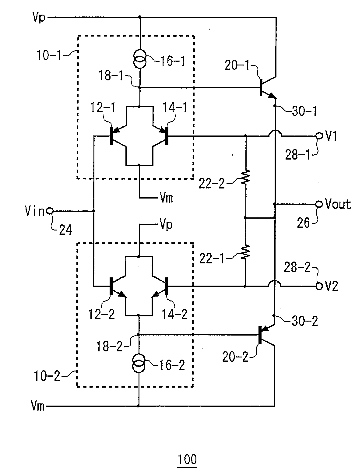
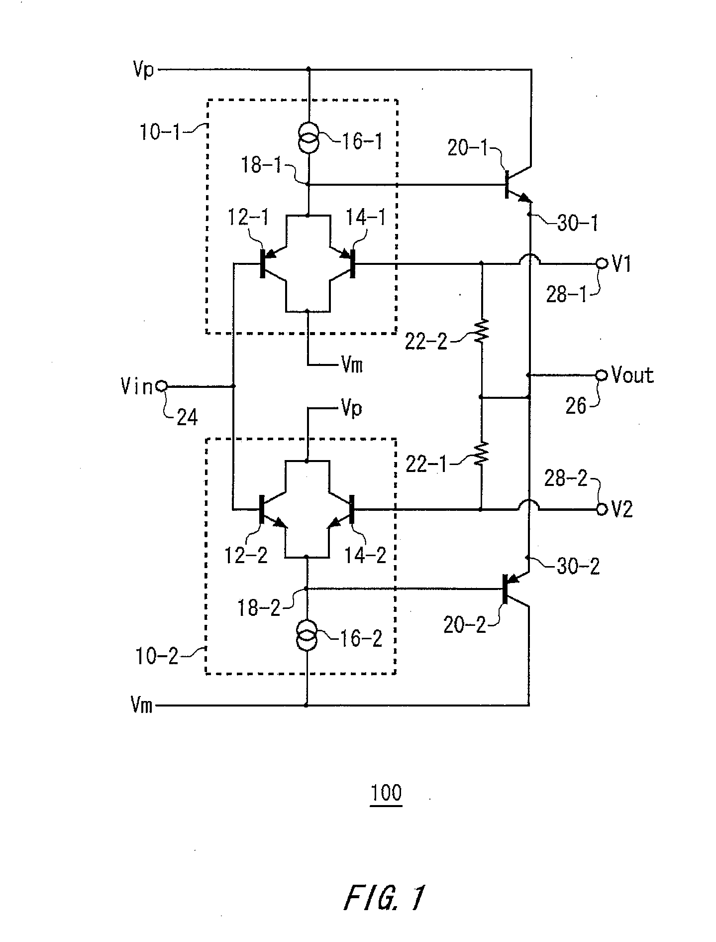
[0025]FIG. 1 is a view exemplary showing a configuration of a buffer circuit 100 according to an embodiment of the present invention. The buffer circuit 100 outputs an output signal according to an input signal. Moreover, the buffer circuit 100 restricts a signal level Vout of the output signal in accordance with a given clamp voltage.

[0026]The buffer circuit 100 includes a first differential-pair circuit 10-1, a second differential-pair circuit 10-2, a first output transistor 20-1, a second output transistor 20-2, a first operation bias resistor 22-1, a second operation bias resistor 22-2, an input terminal 24, an output terminal 26, a first clamp terminal 28-1, and a...


PUM


Abstract

There is provided a buffer circuit that outputs a signal according to an input signal. The buffer circuit includes a first receiving transistor that receives the input signal through its base terminal, a first clamp transistor having polarity same as that of the first receiving transistor, of which an emitter terminal and a collector terminal are connected to corresponding terminals of the first receiving transistor and which receives a first clamp voltage restricting a signal level output from the buffer circuit through its base terminal, and a first current defining section that is commonly provided for the first receiving transistor and the first clamp transistor and defines a total amount of emitter currents flowing into the first receiving transistor and the first clamp transistor. The buffer circuit outputs an output signal according to an emitter voltage of the first receiving transistor.

Description

BACKGROUND[0001]1. Technical Field[0002]The present invention relates to a buffer circuit, an amplifier circuit, and a test apparatus. More particularly, the present invention relates to a buffer circuit that generates an output signal of which a signal level is restricted to a predetermined range, an amplifier circuit that uses this buffer circuit, and a test apparatus that uses this amplifier circuit.[0003]2. Related Art[0004]As a circuit that restricts a level of a signal, there has been known a circuit in which a forward-direction diode and a backward-direction diode are provided between a signal transmission path and a ground potential, for example. Moreover, a resistance is formed on the signal transmission path. Such a circuit can restrict a level of a signal to a range prescribed with forward-direction and backward-direction threshold voltages of the diodes. Moreover, the restriction range of the signal level can be adjusted by serially providing voltage sources in each diod...

Claims


Application Information

Patent Timeline
Patent Type & Authority Applications(United States)
IPC IPC(8): G01R1/30H03K5/08H03G3/20
CPCG01R1/30G01R19/2506H03F3/4508H03K19/01812H03F2203/45552H03F2203/5021H03G11/002H03F3/50
Inventor KIMURA, HIROKI
Owner ADVANTEST CORP
Learn More