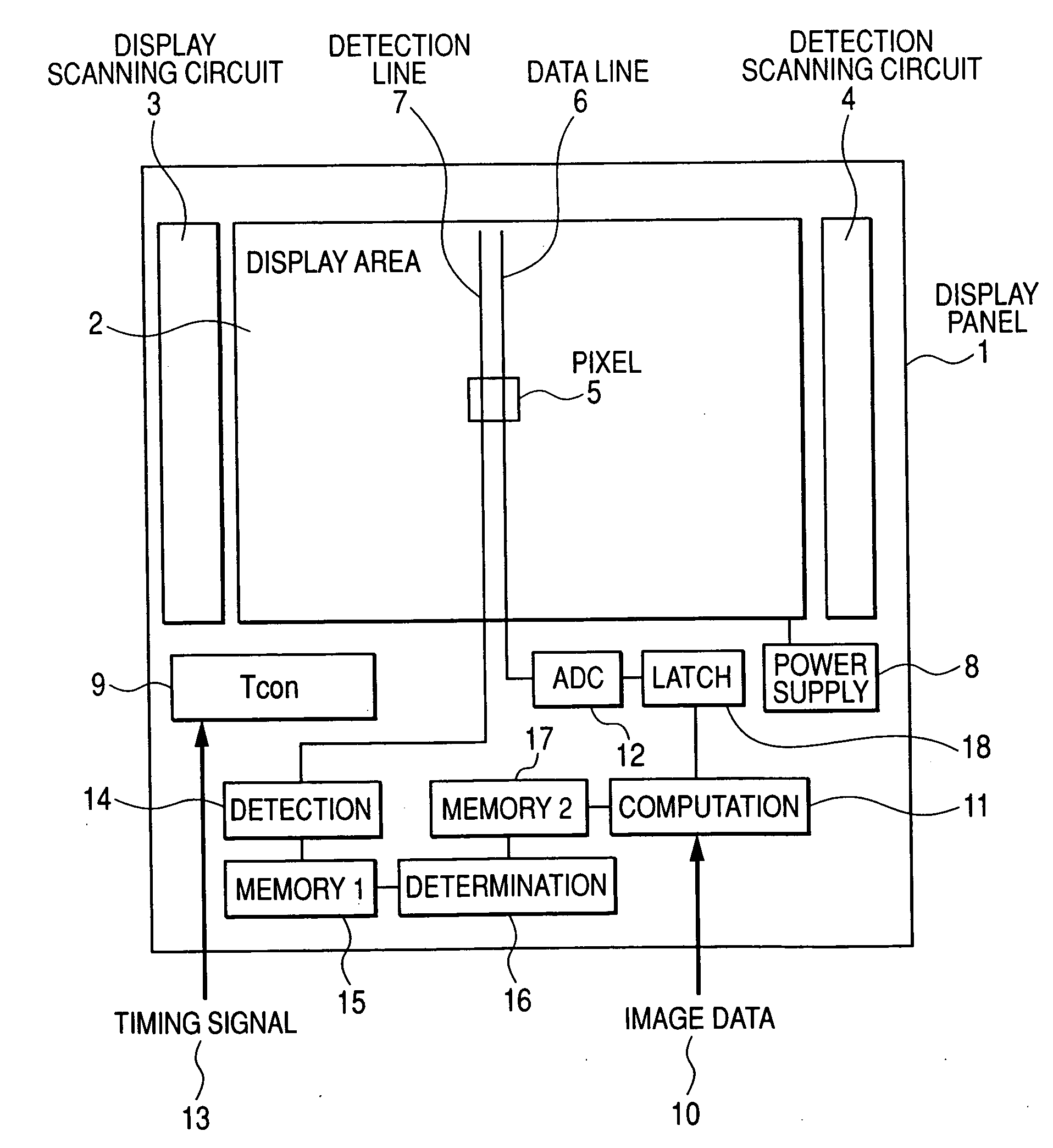
Imaging device

a technology of a display panel and an image, applied in the direction of static indicating devices, instruments, etc., can solve the problems of difficult to compute a precise correction amount, and errors in determining the deterioration, so as to improve the image quality of the display panel using organic el elements, the effect of reducing the probability of burnout and reducing the risk of deterioration

Active Publication Date: 2009-01-29
SAMSUNG DISPLAY CO LTD
View PDF17 Cites 15 Cited by
  • Summary
  • Abstract
  • Description
  • Claims
  • Application Information

AI Technical Summary

Benefits of technology

[0013]If a reference for the determination is set for each position within the display area, the effect of the temperature gradient in the display area and the difference between initial characterist...

Problems solved by technology

However, when the difference of deterioration between the pixels and the reference pixel is computed to correct for burnout, due to the initial difference in characteristics of the pixels and their inherent temperature dependence, it is difficult to compute a precise correction amount.
In particular, since the characteristics of orga...

Method used


Image

  • Imaging device
  • Imaging device
  • Imaging device

Examples


first embodiment

[0040]The prior art embodiment shows a method for detecting a pixel property where it was not necessary to consider the effect of temperature dependence, initial property, etc. of the pixels 5 in the display area. Hereafter, an embodiment will be described where the effect of temperature dependence is taken into consideration. FIG. 7 is a plan view showing a display panel identical to that of FIG. 5 describing the problem when temperature dependence is taken into consideration. FIG. 8 is a voltage-current characteristic diagram illustrative of the temperature dependence of an organic EL element. FIG. 9 is a waveform diagram identical to that of FIG. 6 that changes due to temperature dependence of the organic EL element. When the display panel using the organic EL element is illuminated, the panel temperature rises. In particular, since the temperature rise in the center (high-temperature part) of the display panel 2 is sharp, and there is a low temperature part 33 on the edge of the...

second embodiment

[0048]FIG. 15 is a diagram of essential components describing an imaging device having a function for detecting and determining pixel burnout according to a second embodiment of the invention. According to this embodiment, plural pixels 5 in areas 57 shaded in FIG. 15 are taken as one of the blocks 57, and burnout detection and determination are performed in this block unit. First, the scanning lines G1 to Gm of the area 57 are selected sequentially by the detection scanning circuit 4, and switches the S1 to Si are selected sequentially while one scanning line is selected. To do this, all of the pixels 5 in the block 57 are selected sequentially.

[0049]A fixed current is passed through the selected pixels 5 from the current source. A voltage generated in the organic EL due to this fixed current is input to the buffer amplifier 56, and input to the analog / digital converter ADC 12 at a low impedance. The analog / digital converter ADC 12 converts this voltage to digital data, and stores ...

third embodiment

[0052]FIG. 16 is a diagram of essential components showing an imaging device having a function for detecting and determining pixel burnout according to a third embodiment of the invention. In this embodiment, the block 57 is formed by two adjacent pixels 5 in the scanning line direction shown by a1, a2, a3, a4, . . . , and burnout is determined by comparing with the adjacent pixel. The detection and determination procedure is as follows. First, one scanning line, here the scanning line G1, is selected by the detection scanning circuit 4. While this scanning line G1 is selected, the switches S1 to Sj are switched ON one after another, a fixed current is passed from the current source 54, and the corresponding voltage is stored in the first memory 15 via the buffer amplifier 56 and ADC 12. After the characteristics of all the organic EL elements of the pixels 5 in one scanning line have been detected, the determination circuit 16 performs a comparison with adjacent pixels for the volt...


PUM


Abstract

To determine a deterioration and maintain a high-quality image without unevenness of brightness by performing a precise correction, a detection scanning line for selecting a pixel which detects a deterioration of a pixel, a detection line for informing the outside of the display area of the property of a pixel selected for detecting the deterioration, a deterioration determination means for determining a deterioration amount based on a voltage corresponding to a current detected by the detection line, and a deterioration correction means (computation circuit) for reflecting the determination result of the deterioration determination means in image data supplied to the pixel, are provided.

Description

CLAIM OF PRIORITY[0001]The present application claims priority from Japanese patent application JP 2007-191213 filed on Jul. 23, 2007, the content of which is hereby incorporated by reference into this application.FIELD OF THE INVENTION[0002]The present invention relates to an imaging device using a display panel wherein self-luminous elements are disposed in a matrix array, and in particular relates to an imaging device wherein image quality can be maintained by detecting burnout of the self-luminous elements, and correcting for the burnout.BACKGROUND OF THE INVENTION[0003]An imaging device using a self-luminous display panel formed by self-luminous elements such as organic light emitting diodes (referred to hereafter as OLED) is known. This imaging device using self-luminous display elements has high visibility, does not require an auxiliary lighting device such as a backlight in a liquid crystal panel, and has a high response speed. Organic EL elements which are typical self-lumi...

Claims


Application Information

Patent Timeline
IPC IPC(8): G09G3/30
CPCG09G3/3233G09G2310/0262G09G2320/0233G09G2320/0693G09G2320/0295G09G2320/041G09G2320/048G09G2320/0285
Inventor MIYAMOTO, MITSUHIDEKOHNO, TOHRUISHII, MASATOKASAI, NARUHIKOAKIMOTO, HAJIME
Owner SAMSUNG DISPLAY CO LTD
Why Eureka
Try Eureka