

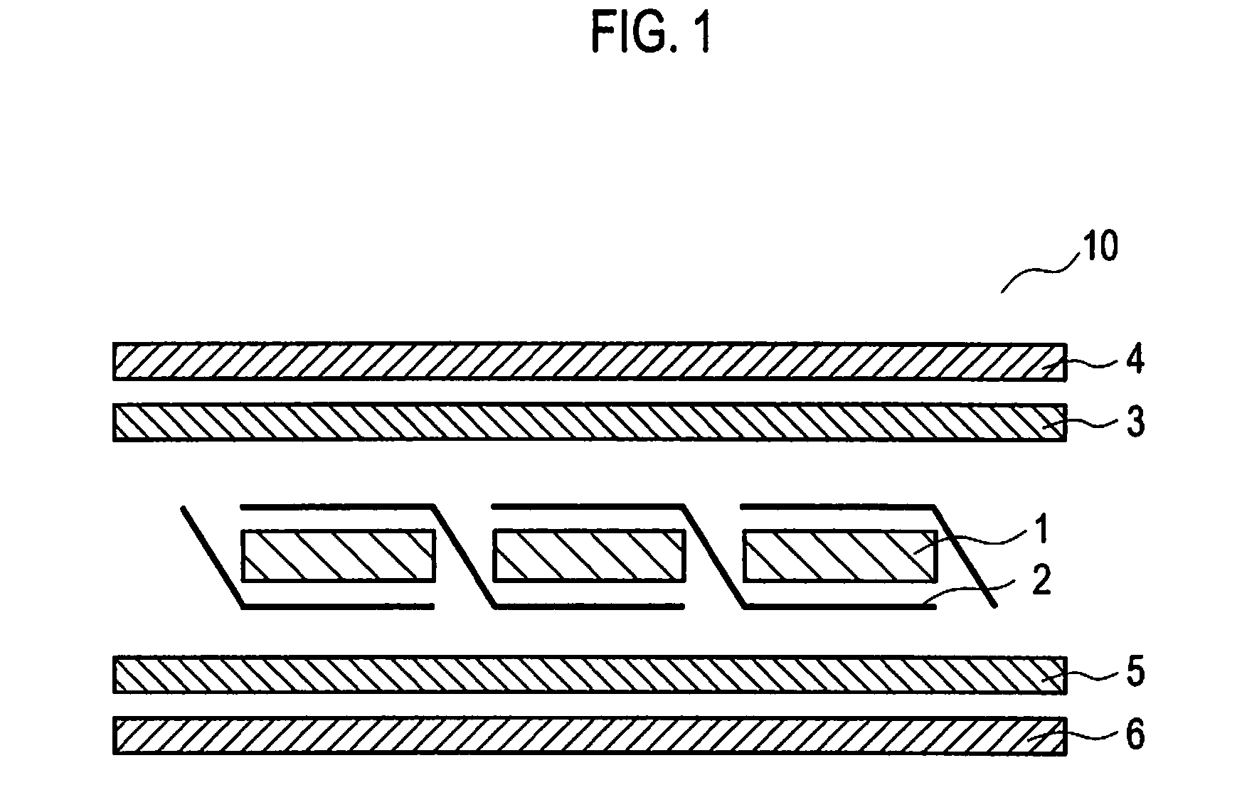
Solar cell module
- Summary
- Abstract
- Description
- Claims
- Application Information
AI Technical Summary
Benefits of technology
Problems solved by technology
Method used
Image

Examples
first embodiment
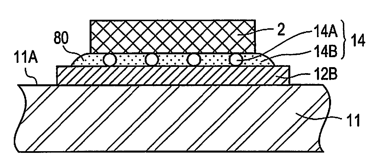
[0053]A solar cell module according to a first embodiment will be described below.
[0054]As shown in FIGS. 4 and 5, in the solar cell module according to the present embodiment, conductive resin adhesive 14 is formed within the surface on wiring material 2 side of connection electrode 12B. In addition, wiring material 2 is arranged so that the top surface of a peripheral portion of conductive resin adhesive 14 would protrude from wiring material 2 to form exposed portion 80.
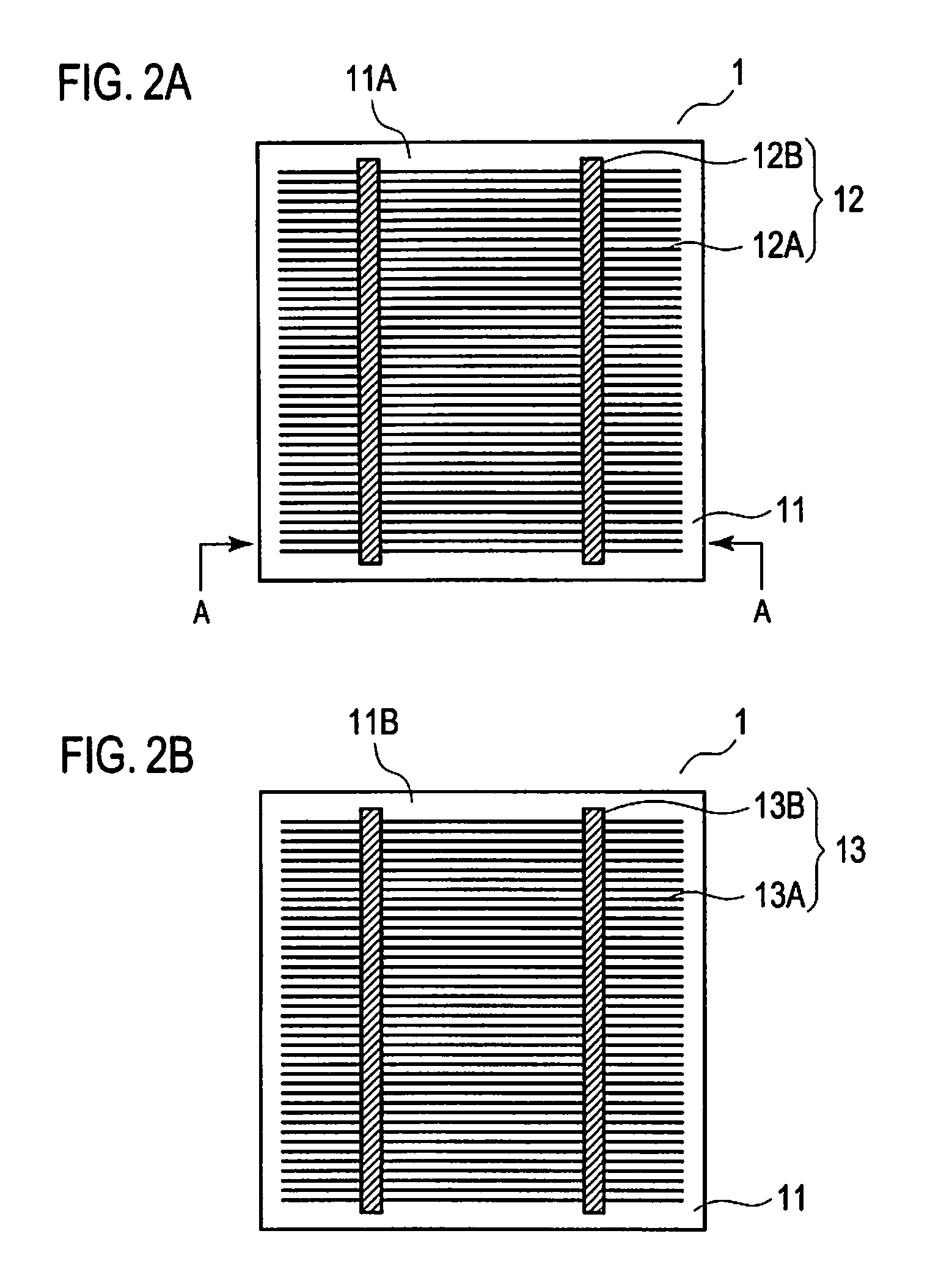
[0055]FIGS. 6 to 8 are views, each of which project onto a projection plane parallel with light-receiving surface 11A, for illustrating regions respectively corresponding to connection electrode 12B, conductive resin adhesive 14, and wiring material 2. Region α surrounded by the solid line in FIG. 6, is a region corresponding to connection electrode 12B. Region β surrounded by the solid line in FIG. 7, is a region corresponding to conductive resin adhesive 14. Region γ surrounded by the solid line in FIG. 8, is a ...
second embodiment
[0059]Next, a solar cell module according to a second embodiment will be described below.
[0060]FIGS. 10A to 10C are each an enlarged plan view of essential parts for illustrating a bonding structure of wiring material 2 by conductive resin adhesive 14. FIG. 11 is a cross-sectional view taken along the C-C line of the enlarged plan view of essential parts shown in FIG. 10A. As shown in FIGS. 10A to 10C and 11, in the solar cell module according to the present embodiment, conductive resin adhesive 14 is formed within the surface on wiring material 2 side of connection electrode 12B. In addition, opening 70 is provided in wiring material 2 for exposing conductive resin adhesive 14 provided thereunder.
[0061]FIGS. 12 to 14 are views projected onto a projection plane that is parallel with light-receiving surface 11A, for illustrating regions respectively corresponding to connection electrode 12B, conductive resin adhesive 14, and wiring material 2. Region α surrounded by the solid line in...
third embodiment
[0064]Next, a solar cell module according to a third embodiment will be described below.
[0065]FIGS. 15A to 15C are each an enlarged plan view of essential parts for illustrating a bonding structure of wiring material 2 by conductive resin adhesive 14. FIG. 16 is a cross-sectional view taken along the D-D line of the enlarged plan view of essential parts shown in FIG. 15A. In the solar cell module according to the present embodiment, as shown in FIGS. 15A to 15C and 16, conductive resin adhesive 14 is formed within the surface on connection electrode 12B side of wiring material 2 and covers an upper surface and side surfaces on wiring material 2 side of connection electrode 12B. In addition, opening 70 is provided in wiring material 2 for exposing conductive resin adhesive 14 provided thereunder.
[0066]FIGS. 17 to 19 are views projected onto a projection plane parallel with light-receiving surface 11A, for illustrating regions respectively corresponding to connection electrode 12B, co...
PUM
 Abstract
Description
Claims
Application Information