

Roll to roll nanoimprint lithography
a nano-imprint and roll-to-roll technology, applied in nanoinformatics, nuclear engineering, polarising elements, etc., can solve the problems of fundamental limitations from the current nil process and the associated throughput (e.g., about several minutes or longer per si wafer) are still far from meeting the demands of most practical applications, and the high-speed imprinting, based on the original nanoimprint scheme, have fundamental limitations. material and process perspectives,
- Summary
- Abstract
- Description
- Claims
- Application Information
AI Technical Summary
Problems solved by technology
Method used
Image

Examples
example 1
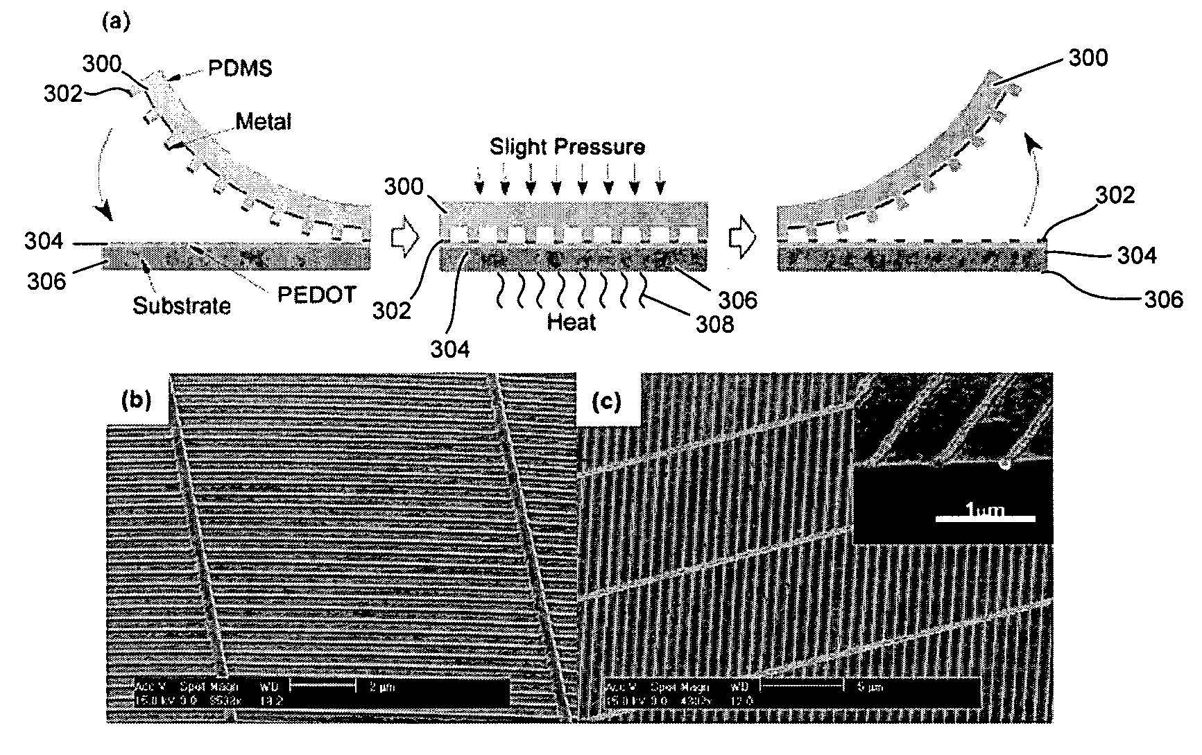
[0103]Example 1 illustrates apparatus and methods for fabricating a bilayer metal wire-grid polarizer using roll-to-roll nanoimprint lithography on a flexible plastic substrate in accordance with the present disclosure.
[0104]A bilayer metal wire-grid polarizer has several advantages over a single-layer wire-grid polarizer and a conventional polarizer, including higher polarization efficiency and easier fabrication. Fabrication of the bilayer metal wire-grid polarizer on a flexible plastic substrate can be achieved using a continuous roll-to-roll nanoimprint lithography (R2RNIL) process. To fabricate the wire-grid polarizer, a subwavelength grating structure in epoxysilicone material is first created on a flexible PET substrate by UV R2RNIL followed by aluminum deposition. Polarizers having an extinction ratio exceeding 1000 can be fabricated.
[0105]The polarizer is an important optical element used in a variety of applications. Wire-grid polarizers in the form of subwavelength metall...
example 2
[0107]Example 2 illustrates apparatus and methods for fabricating an organic solar cell using a nanoimprinted transparent copper electrode in accordance with the present disclosure.
[0108]Cost effective and highly efficient renewable energy is becoming ever more important nowadays to combat the rising price of energy and global climate change. Solar energy is a non-exhaustible and green energy. Organic solar cells (OSC) have the merits of low cost, easy fabrication, and compatibility with flexible substrates over a large area and therefore are considered a promising energy conversion platform for clean and carbon-neutral energy production. The power conversion efficiency of OSC based on conjugated polymers has been steadily increasing through improved energy harvesting, efficient charge separation by the use of donor-acceptor heterojunction structure, and optimization of the processing parameters such as solvent evaporation time and annealing conditions.
[0109]Most organic solar cells...
example 3
[0131]Example 3 illustrates apparatus and methods for fabricating nanoimprinted semitransparent metal electrodes and their application in organic light-emitting diodes in accordance with the present disclosure.
[0132]Organic light-emitting diodes (OLEDs) are promising for full-color, full-motion, flat panel display applications because they offer several advantageous features, for example, ease of fabrication, low cost, light weight, bright self-emission, a wide viewing angle, and the possibility of flexible displays. The basic OLED structure includes a number of organic semiconductor layers sandwiched between a cathode and an anode. For efficient electron injection into the organic layers, low-work-function materials are required for the cathode. A very thin lithiumfluoride (LiF) layer with a thick Aluminum (Al) capping is widely used for this purpose. For the anode, indium tin oxide (ITO) is the predominant choice because it offers transparency in the visible range of the electroma...
PUM
| Property | Measurement | Unit |
|---|---|---|
| surface energy | aaaaa | aaaaa |
| viscosity | aaaaa | aaaaa |
| speed | aaaaa | aaaaa |
Abstract
Description
Claims
Application Information