Organic light emitting display and driving method thereof

a technology of light emitting display and organic light, which is applied in the direction of instruments, measurement devices, static indicating devices, etc., can solve the problems that the organic light emitting display cannot display the image with desired luminance and the image with uniform luminance is not displayed, and achieves uniform luminance

Active Publication Date: 2009-02-26
SAMSUNG DISPLAY CO LTD
View PDF38 Cites 181 Cited by
  • Summary
  • Abstract
  • Description
  • Claims
  • Application Information

AI Technical Summary

Benefits of technology

[0017]It is an aspect according to an exemplary embodiment of the present invention to provide an organic light emitting display and a driving method thereof capable of d

Problems solved by technology

However, there is a problem that such an organic light emitting display cannot display an image with desired luminance due to the efficiency change according to the degradation of the organic light emitting diode OLED.
Also, the c

Method used


Image

  • Organic light emitting display and driving method thereof
  • Organic light emitting display and driving method thereof
  • Organic light emitting display and driving method thereof

Examples


first embodiment

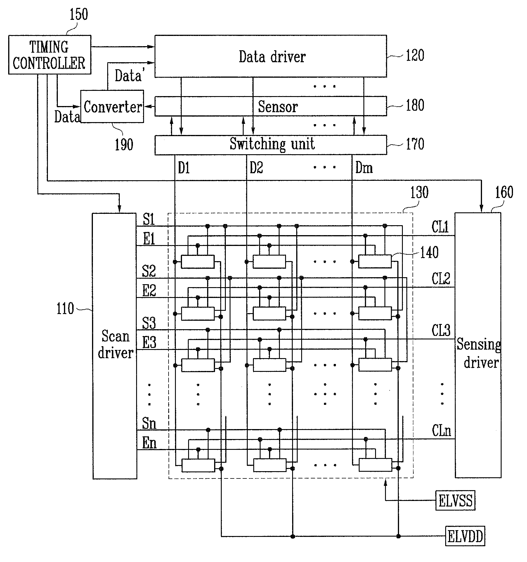
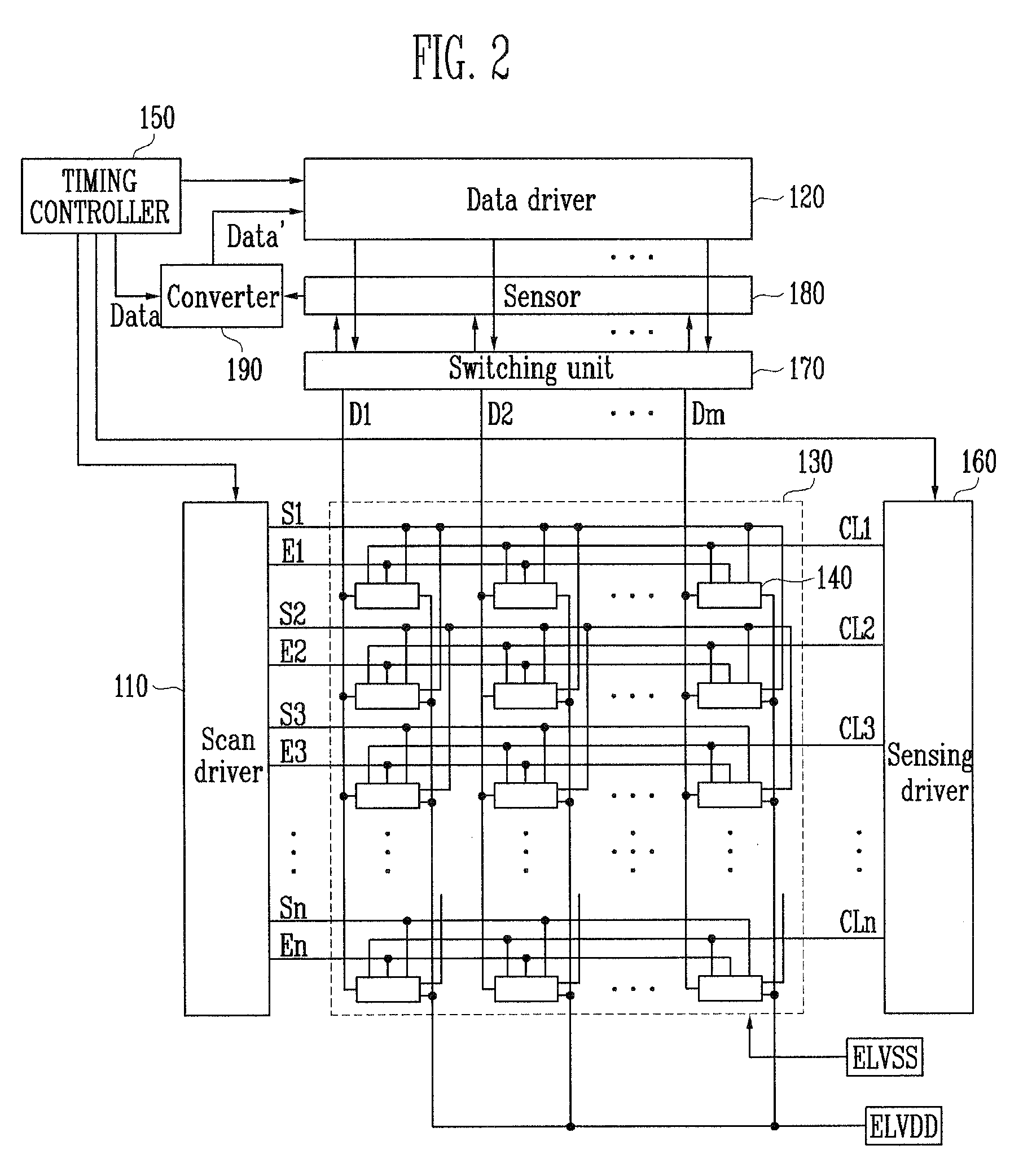
[0048]FIG. 3 shows a pixel shown in FIG. 2. For convenience of description, FIG. 3 shows a pixel coupled to an mth data line (Dm) and an nth scan line (Sn).

[0049]Referring to FIG. 3, the pixel 140 according to the first embodiment of the present invention includes an organic light emitting diode OLED and a pixel circuit 142 for supplying current to the organic light emitting diodes OLED.

[0050]The anode electrode of the organic light emitting diode OLED is coupled to the pixel circuit 142 and the cathode electrode of the organic light emitting diode OLED is coupled to the second power supply ELVSS. The organic light emitting diodes OLEDs generates light corresponding to current supplied from the pixel circuit 142.

[0051]The pixel circuit 142 is supplied with the data signal supplied to the data line Dm when the scan signal is supplied to the scan line Sn. Also, the pixel circuit 142 provides the degradation information of the organic light emitting diodes OLEDs and / or the mobility inf...

second embodiment

[0061]FIG. 4 shows a pixel shown in FIG. 2. For convenience of description, FIG. 4 shows a pixel coupled to an mth data line (Dm) and an nth scan line (Sn).

[0062]Referring to FIG. 4, the pixel 140′ according to the second embodiment of the present invention includes an organic light emitting diode OLED and a pixel circuit 142′ for supplying current to the organic light emitting diodes OLED. The pixel 140′ according to the second embodiment is different from the pixel 140 according to the first embodiment shown in FIG. 3 in that the pixel circuit 142′ includes seven transistors M1′ to M7′, two capacitors C1′ and C2′, and one switching element T1.

[0063]In the pixel circuit 142′, the gate electrode of the first transistor M1′ is coupled to the scan line Sn and the first electrode of the first transistor M1′ is coupled to the data line Dm. The second electrode of the first transistor M1′ is coupled to a first node A.

[0064]The gate electrode of the second transistor M2′ is coupled to a s...


PUM


Abstract

An organic light emitting display device includes: a plurality of pixels at crossing portions of data lines, scan lines, and emission control lines; a sensor for sensing degradation information of organic light emitting diodes and mobility information of driving transistors, which are included in each pixel; a converter for storing the degradation information of organic light emitting diodes and the mobility information of driving transistors, which are sensed utilizing the sensor and converting input data to corrected data by utilizing the stored information; and a data driver receiving the corrected data and generating data signals to be supplied.

Description

CROSS-REFERENCE TO RELATED APPLICATIONS[0001]This application claims priority to and the benefit of Korean Patent Application No. 10-2007-0084730, filed on Aug. 23, 2007, in the Korean Intellectual Property Office, the entire content of which is incorporated herein by reference.BACKGROUND[0002]1. Field of the Invention[0003]The present invention relates to an organic light emitting display and a driving method thereof, and in particular to an organic light emitting display and a driving method thereof capable of displaying an image with substantially uniform luminance.[0004]2. Discussion of Related Art[0005]Recently, various flat panel display devices having reduced weight and volume, which are disadvantages of cathode ray tubes, have been developed. Types of flat panel display devices include a liquid crystal display (LCD), a field emission display (FED), a plasma display panel (PDP) and an organic light emitting display, etc.[0006]An organic light emitting display among the flat p...

Claims


Application Information

Patent Timeline
IPC IPC(8): G09G3/30
CPCG09G3/3233G09G3/3283G09G2300/0814G09G2300/0819G09G2300/0852G09G2320/0295G09G2310/027G09G2310/0272G09G2320/0233G09G2320/043G09G2320/045G09G2300/0861G09G3/30G09G3/32G01R19/00G09G3/20
Inventor KWON, OH-KYONG
Owner SAMSUNG DISPLAY CO LTD
Why Eureka
Try Eureka